 電子發燒友App


Using the MAX4196 instrumentation amplifier (IA) as a pre-amplification circuit, adds a factor of 10V/V gain to the signal path enabling low output strain gauge sensors to be temperature compensated and calibrated. Complete circuits for high-gain amplification and temperature compensation of such sensors will be presented and discussed.
Pressure sensors and force sensors that use thin-film or thick-film (TF) strain gauge technology typically require signal amplification of several hundred volts per volt. The sensor signal must be compensated for changes in offset and span due to temperature changes.
The MAX1452 Precision Sensor Signal Conditioner provides all of the functions required for sensor bridge excitation (offset and span temperature compensation, and output offset adjustment with 16-bit trim resolutions). However, the MAX1452 design was optimized for piezo-resistive transducers (PRT), silicon micro-machined devices which typically require low signal gain due to their high bridge sensitivity.
The MAX1452 has a selectable gain range of 39-234V/V. PRT sensors can have full-scale (FS) output signal levels of 20-40 mV/V1 and thus require a gain in the range of 42-83V/V when using 3V of bridge excitation voltage to produce an output voltage swing of 5V. TF sensors typically have much lower bridge sensitivity levels of 1.5 to 2.5 mV/V and thus require gains of 360-830V/V with a bridge excitation voltage of 4V to produce a 5V output swing.
Using the MAX4196 instrumentation amplifier (IA) as a pre-amplification circuit adds a factor of 10V/V gain to the signal path enabling TF sensor calibration and temperature compensation with the MAX1452. A complete circuit for amplifying and temperature compensating a TF sensor using this architecture is shown in Figure 1.
Figure 1. The MAX4196 IA amplifies the sensor signal by a fixed gain of 10.
The MAX4196 was chosen2 for its internally set fixed gain of 10 and requires no external components other than a bypass capacitor on the power supply. The op-amp in the MAX1452 is used to set an arbitrary mid-rail voltage of 2.5V to provide a reference signal to the MAX4196 REF input and to the MAX1452 INM input. The differential sensor signal is converted to a single-ended signal at the MAX4196 OUT pin with respect to the REF pin. The MAX1452 differential input is driven by this single-ended signal into the INP pin with respect to the INM input.
This provides a bipolar signal swing of the sensor signal about a zero-point set by the op-amp and resistor divider formed by the 47KΩ resistors. For sensors that have a positive offset at no-load and only swing in the positive output direction (such as typically found in weight sensor applications), the op-amp and resistor circuit can be eliminated by tying the MAX4196 REF and the MAX1452 INM pins directly to VSS. This is shown in Figure 2.
Figure 2. Unidirectional sensor connections.
The MAX1452 provides the bridge excitation for the sensor bridge. The excitation source is limited to 2mA in drive current capability when configured as a current source for PRT devices, but can deliver as much as 4mA of current when wired as a voltage excitation source (Pins BDR and ISRC connected together) and even higher currents with additional circuitry. With this current drive capability, TF sensors with bridge resistances as low as 1200Ω can be driven with excitation voltages of 4.5V. Since TF sensors typically have a very low temperature coefficient of resistance (TCR) and temperature coefficient of sensitivity (TCS) of the bridge, the excitation voltage does not require much compensation adjustment range and thus can be set to a value near the upper supply rail (typically VBDR = 4.5V). The higher the excitation voltage, the lower the required signal gains.
There are 16 gain settings for the MAX1452 that range from 39 to 234 in increments of 13. This range is expanded to 390 to 23403 in increments of 130. The calibrated gain of the overall circuit is also a function of the bridge excitation voltage, VBDR, as shown in the following equation:
VOUT = BridgeOutput(mV/V) × VBDR(V) × GMAX4196(V/V) × GMAX1452(V/V)
In order to have a continuous gain selection range, it is important that the fixed gain steps of the circuit overlap when using reasonable excitation voltages. A reasonable range of excitation voltages for TF sensors is 3.0-4.5V. The lower limit of 3.0V is imposed by consideration of system noise and the upper limit of 4.5V is imposed by the bridge excitation source requiring VBDR to be 0.5V below VDD for compliance or headroom for circuit operation. The overlapping gain selection ranges is shown graphically in Figure 3.
Figure 3. The overall selectable gain ranges provide overlap with various sensor outputs.
Since the MAX1452 modulates the bridge excitation voltage as a means to adjust the overall gain for compensation of span over temperature, it is important to look at this effect on the MAX4196 pre-amplifier. Typical TF sensors have very good TCS performance and may vary by only a few percent over a 100°C temperature range. This requires that the bridge excitation be varied by only a few percent, typically only Δ150mV, over the same temperature range in order to compensate the effect. This small change in VBDR will produce a small change in the common mode output voltage into the MAX4196. The MAX4196 provides a common-mode rejection of 88dB minimum over the operating range of -40°C to 85°C. At an overall system gain of 910V/V (worst-case calculations is at high gains) this translates into an output error signal of 0.1%.
An additional bonus of this increased gain architecture over those circuits that use a gain stage on the output of the MAX1452 is a significant improvement in noise performance. The MAX1452 programmable gain amplifier (PGA) is a switched capacitor architecture that generates a small, but significant, output noise. This noise level scales (non-linearly) with the PGA gain setting. Higher PGA gain settings produce a higher output noise. Placing the additional gain circuitry at the input to the MAX1452, and using the lower PGA gain settings can realize a high signal gain system.
Notes
1Sensors wired in the Wheatstone bridge configuration are typically rated in millivolts of differential output signal per volt of bridge excitation voltage applied at the rated full-scale load of the sensor. Hence, a sensor rated at 2mV/V output at full-scale load will produce 8mV of differential output voltage when excited with 4V and full-scale load applied.
2The MAX4194 IA could be used equally well and provides a user-settable gain with the addition of an external gain setting resistor.
3Gains in excess of 1000 become dominated by system noise and are not suitable for general applications.
高增益的信號調理電路的薄膜和厚膜傳感器-High-Gain
Abstract: Sensors that use thin-film or thick-film strain gauge technology typically require high-gain signal conditioning. For typical applications where signal gain of less than 250V/V is sufficient, any of the high precision signal conditioners, MAX1452, MAX1455, MAX1457, and MAX1463 ASICs can be used without any external amplification of the signal. For applications where high-gain compensation (larger than 250V/V) is required, external amplification circuit must me added.
- 傳感器(788346)


相關推薦
熱點推薦
非標準化溫度傳感器信號調理電路的匹配方法和優勢分析
對于具有標準化分度號的傳感器,目前,市場上一般有與之對應的標準化信號調理電路。由于這些標準化信號調理電路是標準設計、批量生產的,因此,其可靠性高,價格一般也較為合理。但具有標準化分度號的傳感器在整個
2020-07-14 07:56:00 3527
3527
3527
薄膜電阻與厚膜電阻的差異
薄膜電阻與 厚膜電阻的共同特征在于,通過在耐熱基板的表面,涂覆一層薄膜狀的電阻材料而形成的電阻元件。薄膜與厚膜最直觀的差異就是這層“膜”(導電層)的厚度。厚膜電阻膜的厚度可以是薄膜電阻的上千倍。
2024-01-18 09:55:433114
3114
傳感器 信號調理電路 的阻容器件 如何選用 ?
本帖最后由 shawshank136 于 2017-3-14 15:06 編輯
傳感器 信號調理電路 的阻容器件 如何選用 ?見附圖,傳感器P3的輸出(輸出_P、輸出_N),經信號調理電路(由
2017-03-14 15:00:57
傳感器電路的低噪聲信號調理
傳感器電路的低噪聲信號調理隨著模數轉換器和數模轉換器分辨率的提高以及電源電壓的降低,最低有效位(LSB)變得更小,這使得信號調理任務變得更加困難。由于信號大小更接近于本底噪聲,因此,必須對外部和內部噪聲源(包括Johnson、散粒、寬帶、閃爍和EMI)進行處理。
2009-12-16 11:00:05
傳感器電路的低噪聲信號調理(第二部分)
。 圖1 所示的是典型信號調理電路中的噪聲源,以及可用于反相、同相、差分及其它通用配置的通用公式。 正確的設計方法 從傳感器及其特征噪聲、阻抗、響應和信號幅度入手,實現最低的折合到輸入端(RTI
2018-11-02 15:44:33
傳感器到底需要什么樣的電路板
傳感器則是通過沉積在介質襯底(基板)上的,相應敏感材料的薄膜形成的。使用混合工藝時,同樣可將部分電路制造在此基板上。 厚膜傳感器是利用相應材料的漿料,涂覆在陶瓷基片上制成的,基片通常是Al2O3制成
2018-11-08 15:45:17
信號調理電路的設計(設計調理方案+電路解析)
幫助您直接連接到廣泛的傳感器和信號類型(從熱電偶到高電壓信號)來實現的。關鍵的信號調理技術可以將數據采集系統的總體性能和精度提高10倍。信號調理簡單的說就是將待測信號通過放大、濾波等操作轉換成采集設備能夠識別的標準信號。是指利用內部的電路(如濾波器、轉換器、放大器等…)來改變輸入的訊號類型并輸出之。
2019-01-07 15:46:56
厚膜電阻材料常用的有哪些
溫度系數和噪音層面存在的問題,不適感用以高精密及數據信號的電源電路。
二、厚膜電阻器
厚膜電阻是把金屬材料類電阻器原材料與有機化學填充料混合起來包裝印刷后燒制,還能夠在其上包裝印刷保護層厚度
2024-03-13 06:56:09
厚膜集成電路的技術原理相關資料分享
、STR59041等型號。它激式開關電源電路中常用的厚膜集成電路有STR-S6708、STR-S6709等型號。 2.音頻功放厚膜集成電路 音頻功放集成電路的主要作用是對輸入的音頻信號進行功率放大
2021-05-26 06:58:08
高增益低噪聲的探測器讀出電路設計
是微光CMOS圖像傳感器的重要組成部分,它的基本功能是將探測器微弱的電流、電壓或電阻變化轉換成后續信號處理電路可以處理的電信號,它的噪聲水平限制著CMOS圖像傳感器在微光下的應用。微光條件下像素的輸出
2018-11-12 15:59:07
ICP傳感器信號調理電路
求大佬。設計了一個ICP加速度傳感器恒流源供電以及信號調理電路,如圖,制作出來的電路板測得有4mA電流和24V電壓,但是傳感器沒有輸出是怎么回事呀?
2023-09-18 18:16:37
ICP振動傳感器信號調理電路(放大電路)設計?
` 本帖最后由 zhongjian110 于 2020-12-22 21:27 編輯
各位大俠們,本人對電子信號調理電路涉及甚少,目前遇到ICP振動傳感器信號調理電路(放大電路
2020-12-22 21:17:29
麗智高壓厚膜貼片電阻-阻容1號
等領域。它可以用于電源和過濾電路中,以提供較高的電壓和電流承受能力。此外,在各種電子設備中,如工業自動化控制系統和敏感傳感器等應用場景中也可以使用高壓厚膜貼片電阻。
特性Features
2023-05-16 16:50:29
基于厚膜力傳感器的便攜式電子秤能實現什么功能?
基于厚膜力傳感器的電子秤設計介紹一種基于厚膜力傳感器和利用AT89C52單片機等器件設計的便攜式電子秤。該電子秤能對3kg量程范圍內的物體進行稱量,能實現去皮、清零/復位、計價、超重報警等功能。?
2020-04-20 06:15:15
基于壓電薄膜(PVDF)傳感器以及無線傳輸的振動信號測量系統
為了滿足振動傳感器陣列對多點信號實時傳輸的要求,研制了一種基于壓電薄膜(PVDF)傳感器以及無線傳輸的振動信號測量系統。該系統包含振動信號采集模塊及主控單元,前者集成了振動信號調理電路
2020-08-26 08:04:16
干涉型光纖擾動傳感器信號調理電路怎么設計?
在現代傳感系統中,干涉型光纖擾動傳感器以其極高的靈敏度得到了廣泛關注。其中關鍵部分是信號調理電路,它用來檢測和預處理非常微弱并夾雜著噪聲的傳感信號。一般來說,光電探測器的輸出信號要先經過前置
2020-03-10 06:54:31
干涉型光纖擾動傳感器微弱傳感信號的調理電路怎么設計?
在現代傳感系統中,干涉型光纖擾動傳感器以其極高的靈敏度得到了廣泛關注。其中關鍵部分是信號調理電路,它用來檢測和預處理非常微弱并夾雜著噪聲的傳感信號。一般來說,光電探測器的輸出信號要先經過前置
2020-03-10 06:16:37
怎么區分電阻是薄膜式還是厚膜式?
薄膜電阻和厚膜電阻是使用較多的一種類型電阻,薄膜電阻是現在主流的貼片精密電阻器,但是如何區分這兩種電阻呢? 1、根據膜厚 厚膜電阻的膜厚一般大于10μm,薄膜的膜厚小于10μm,大多處于小于1μm
2018-12-05 20:18:08
怎么區分電阻是薄膜還是厚膜
要區分電阻是薄膜還是厚膜,可以從以下幾個方面進行判斷:
外觀:觀察電阻的外觀,如果看到電阻表面有一層薄膜涂層,則可能為薄膜電阻;如果電阻表面較為粗糙,沒有明顯的涂層,則可能為厚膜電阻。
尺寸:薄膜
2024-03-07 07:49:07
怎么完成多種溫度傳感器信號調理工作?
難滿足精度,因此需選用不同類型的傳感器,然而考慮到重量后就很難選出合適的傳感器來,因此本文旨在一片電路板上完成多種傳感器的信號調理工作,該設計有較大的實際意義。
2020-04-08 06:14:28
求壓電加速度傳感器以及電渦流傳感器的信號調理電路,.....
我的畢業設計課題是精密機床半主動減振系統設計,其中要涉及到壓電加速度傳感器和電渦流傳感器的信號調理電路圖,希望各位前輩們幫幫忙,剛用multisim,不是很了解。。
2013-03-22 12:05:14
液位傳感器的信號調理電路設計
---本文介紹的液位傳感器的信號調理電路以及各種變送器的變換電路是作者實際工作的總結,用該方法設計的液位變送器,經多年的實際應用,證明用該設計方法制作的變送器性能優良運行可靠。:
2018-11-14 14:53:11
電阻傳感器信號調理電路
16 位數/模轉換器(DAC)實現數字化校正,對信號的零位和幅值進行校準,將可以賦予傳感器產品真正的可互換性。國內能做出此類傳感器調理電路的寥寥無幾,有的更是受制于自身芯片設計的缺陷,導致其算法與進口
2020-04-28 15:22:49
請問傳感器信號調理電路的阻容器件怎么選用?
見附圖,傳感器P3的輸出(輸出_P、輸出_N),經信號調理電路(由 兩個電阻、三個電容 組成)后輸入 模數轉換器U6。信號調理電路選用 低溫票、高精度的阻容器件,如下:電阻(低溫票):阻值封裝精度
2019-05-20 02:56:18
超薄片式厚膜電阻
的電阻范圍比薄膜電阻器寬,從幾歐姆到幾G歐不等,可根據用戶要求制定不同的電阻值。
2.輸出功率高:厚膜電阻器具有更高的輸出功率,可以承受更大的電流和功率,這使得它們在大功率應用中更加可靠和穩定。
3
2024-03-15 07:17:56
采用信號調理IC驅動應變片電橋傳感器
轉換器)、溫度傳感器和溫度系數表來完成電橋傳感器的溫度補償和線性化(圖4)。在傳感單元和電壓輸出之間通過模擬信號通路來完成溫度補償和放大。該IC借助很少的外部電路就可以適應金屬片或者厚膜應變片,為惠斯通
2018-11-15 16:21:28
光電測速傳感器及其信號調理電路
介紹了光電測速傳感器的組成,分析了該傳感器的工作原理。在分析該傳感器信號的基礎上,用SD2380 動態分析儀作了頻譜分析。設計了相應的信號調理電路,并據此制作了車速儀,其準確
2009-07-03 09:40:59 366
366
366光電測速傳感器及其信號調理電路
介紹了光電測速傳感器的組成,分析了該傳感器的工作原理。在分析該傳感器信號的基礎上,用SD2380 動態分析儀作了頻譜分析。設計了相應的信號調理電路,并據此制作了車速儀,其準
2009-07-03 09:46:1730
30混合厚膜電路
在現代電子技術領域內,電路設計師經常要接觸到混合微電路。混合微電路一般可分為多片混合電路(MCU)、混合薄膜電路(Hybrid Thin Film Microcircuits)、混合厚膜電路(Hybrid Thick Film M
2010-04-23 08:19:0122
22
High-Gain Signal Conditioning
high-gain signal conditioning. For typical applications where signal gain of less than 250V/V is sufficient, any of the high precision signal cond
2009-04-20 16:15:321013
1013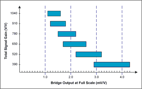
基于厚膜力傳感器的電子秤設計
基于厚膜力傳感器的電子秤設計
介紹一種基于厚膜力傳感器和利用AT89C52單片機等器件設計的便攜式電子秤。該電子秤能對3kg量程范圍內的物體進行
2009-10-13 00:15:441602
1602
厚膜集成電路,厚膜集成電路是什么意思
厚膜集成電路,厚膜集成電路是什么意思
用絲網印刷和燒結等厚膜工藝在同一基片上制作無源網絡,并在其上組裝分立的半導體器件芯
2010-03-20 16:17:261133
1133摩托車油量傳感器用厚膜電路產品說明書
JTB 系列傳感器用厚膜電路是本公司專門為各種摩托車油量檢測 傳感器設計的厚膜電路板。該系列產品耐燃(汽、柴)油、鹽化霧等 工業環境的腐蝕能力強,具有輸出線性特性好、抗磨性能強,使用壽 命長、成本低廉等特點。
2011-03-15 15:52:0463
63ZSSC3170汽車傳感器信號調理電路分析
ZMDI公司的ZSSC3170是集成了脈寬調制接口的汽車傳感器信號調理器,最大模擬增益420,并具有擴展的失調補償。
2011-05-14 09:41:023810
3810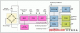
用于薄厚膜傳感器的高增益信號調理電路
使用max4196儀表放大器(IA)作為前置放大電路增加為10V的/ V因子增益信號路徑使TF的MAX1452傳感器校準和溫度補償。一個完整的電路,用于放大和溫度補償的TF傳感器使用這種架構如圖1所示。
2017-04-07 16:50:5611
11碳膜電阻分薄膜和厚膜嗎_如何辨別薄膜電阻與厚膜電阻
厚膜電路一般采用絲網印刷工藝,薄膜電阻采用的是真空蒸發、磁控濺射等工藝方法。厚膜電阻一般精度較差,10%,5%,1%是常見精度,而薄膜電阻則可以做到0.01%萬分之一精度,0.1%千分之一精度等。
2018-01-24 08:57:1016325
16325壓電薄膜傳感器_壓電薄膜傳感器OFweek Mall介紹
命體征監測中的典型應用。當拉伸或彎曲一片壓電聚偏二氟乙烯PVDF聚合物膜(壓電膜)時,在壓電薄膜傳感器膜的上下電極表面之間會產生電信號(電荷或電壓),并且該變形與拉伸或彎曲。按比例。典型的壓電材料對壓力敏感
2018-06-29 14:29:13907
907薄膜電阻器與厚膜電阻器的老化電阻漂移有何區別
Q1:薄膜電阻器與厚膜電阻器的老化電阻漂移有何區別?A:薄膜與厚膜的電阻漂移(老化) 薄膜技術電阻器的老化行為或漂移與厚膜技術電阻器不盡相同。正如下文進一步說明的,厚膜并非均質層。此外,對于厚膜來說
2021-10-11 15:26:313814
3814薄膜電阻與厚膜電阻有何差異?本文一次給你講透!
單單理解到 “膜”(導電層)的厚度的差異,在我們在設計電路以及選擇電阻時,依舊不知道該怎么下手。今天就從三個方面:精度與功率、電流噪聲、溫度系數,來把 薄膜電阻 厚膜電阻 的差異給講透。 精度與功率 上 的差異 概括
2022-12-15 09:30:0211625
11625RTD傳感器信號調理電路簡介
應用中不同信號調理電路的基礎知識。 使用分壓器進行 RTD 測量 可以使用簡單的電阻分壓器將RTD電阻的變化轉換為電壓信號。圖1顯示了鉑RTD的典型電路圖。圖中的Pt1000表示鉑RTD,在0°C時的標稱電阻為1000 Ω。 圖1. 鉑RTD電路圖示例。 與大多數電阻式傳感器一樣
2023-01-27 16:21:004542
4542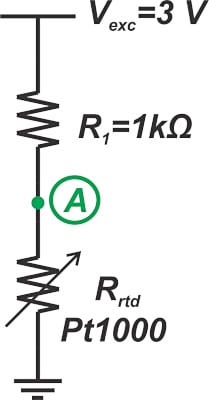
用于薄膜和厚膜傳感器的高增益信號調理電路
使用MAX4196儀表放大器(IA)作為前置放大電路,為信號路徑增加10V/V增益,使低輸出應變計傳感器能夠進行溫度補償和校準。將介紹和討論用于此類傳感器的高增益放大和溫度補償的完整電路。
2023-05-17 11:47:062289
2289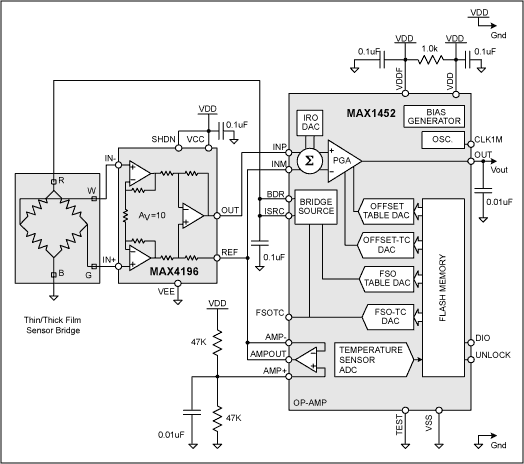
傳感器厚膜工藝術的原理及制備方法
隨著科技的不斷發展和進步,傳感器技術也在不斷創新和改進。其中,傳感器厚膜工藝術是一種比較新的工藝,具有廣泛的應用前景和市場需求。本文將從傳感器厚膜工藝術的定義、原理、制備方法、特點、應用等方面進行探討。
2023-06-07 09:20:141947
194710184000-01壓電薄膜傳感器的信號調理電路
10184000-01壓電薄膜傳感器的輸出信號能量不僅非常微弱,而且內阻非常高,而且輸出能量很小,因此其測量電路通常需要連接一個高輸入阻抗的前置放大器。 它的作用是:一種是將其高輸出阻抗轉換為低
2023-06-02 10:25:271527
1527
薄膜和厚膜電阻有什么區別?
▼關注公眾號: 工程師看海▼ 網絡文章,出處 不詳 什么是后膜電阻和薄膜電阻 薄膜和厚膜電阻器是市場上最常見的類型。它們的特征在于陶瓷基底上的電阻層。雖然它們的外觀可能非常相似,但它們的性能和制造
2023-08-02 08:41:332515
2515
薄膜電阻和厚膜電阻的區別
薄膜電阻和厚膜電阻的區別1.結構:-薄膜電阻:薄膜電阻是通過在絕緣基板上沉積金屬或合金薄膜形成的。常用的薄膜材料有鉑、鎳鉻合金等。薄膜通常具有光滑且均勻的厚度,形成電阻元件的形狀和尺寸是通過光刻
2023-09-15 11:07:4010166
10166
厚膜晶片電阻和薄膜晶片電阻有什么區別?
電阻器是電子電路中常見的被動元件,用于限制電流、調整電壓和執行其他電阻性功能。在電阻器的制造中,有兩種常見的類型:厚膜晶片電阻和薄膜晶片電阻。這兩種類型的電阻器在結構、性能和應用方面都有一些顯著的區別。本文將介紹厚膜晶片電阻和薄膜晶片電阻的區別,以幫助讀者更好地理解它們的特性和用途。
2023-10-23 09:00:172820
2820
薄膜電阻器和厚膜電阻器之間有哪些差異呢?
薄膜電阻器和厚膜電阻器之間有哪些差異呢? 薄膜電阻器和厚膜電阻器是常見的電子元件,用于電路中的精確電阻調節和限流。它們的差異主要體現在制作工藝、性能特點、適用范圍等方面。 第一段:介紹電阻器
2024-01-30 17:26:501916
1916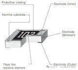
薄膜和厚膜的區別以及不同的制備工藝介紹
相對于塊體材料,膜一般為二維材料。薄膜和厚膜從字面上區分,主要是厚度。薄膜一般厚度為5nm至2.5μm,厚膜一般為2μm至25μm,但厚度并不是區分薄膜和厚膜的標準。
2024-02-28 11:08:516428
6428薄膜在線測厚:精準、高效的理想選擇
技術簡介 薄膜在線測厚技術是一種通過無損測量方式獲取薄膜厚度的技術,其基本原理是使用電磁或光學傳感器對薄膜進行實時厚度測量。這種技術不僅能夠提供準確的厚度數據,而且可以在生產過程中直接進行,無需額外的采樣和
2024-04-17 16:25:55937
937貼片薄膜電阻和厚膜電阻的區別
在電子技術的世界里,電阻器是電子電路中不可或缺的元件之一。其中,貼片薄膜電阻和厚膜電阻作為兩種常見的電阻器類型,各自具有獨特的特點和應用場景。本文將對這兩種電阻器進行詳細的分析和比較,旨在揭示它們之間的區別和聯系。
2024-05-22 15:23:174419
4419薄膜電阻與厚膜電阻的主要區別及其優點
薄膜電阻與厚膜電阻是兩種不同的電阻器類型,它們在材料、制造工藝、性能和應用方面存在一些顯著的區別。 一、薄膜電阻與厚膜電阻的定義 薄膜電阻:薄膜電阻是一種采用薄膜技術制造的電阻器,其電阻體是由薄膜
2024-08-19 15:09:504985
4985如何辨別薄膜電阻與厚膜電阻?
辨別薄膜電阻與厚膜電阻,可以從以下幾個方面進行: 一、外觀與尺寸 外觀:觀察電阻的外觀,如果電阻表面有一層薄膜涂層,可能為薄膜電阻;而厚膜電阻表面則較為粗糙,沒有明顯的涂層。 尺寸:薄膜電阻的尺寸
2024-11-18 15:12:211933
1933
薄膜電阻和厚膜電阻區別介紹
在電子電路設計中,選擇合適的電阻類型對于確保電路的性能和可靠性至關重要。厚膜電阻和薄膜電阻作為兩種常見的電阻類型,它們在制造工藝、精度、電流噪聲和溫度系數等方面有著顯著的差異。 制造工藝和結構
2024-11-24 16:05:112540
2540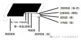
傳感器信號調理應用筆記中的關鍵電路
在傳感器技術中,精確的信號調理對于可靠的數據分析至關重要。放大、相位控制和降噪是這一過程的關鍵環節。本應用筆記探討傳感器信號調理核心的五個基本放大器電路。從反相和同相放大器到精密儀表放大器和多功能差動放大器,每種電路都能獨特地增強傳感器數據。
2025-02-21 09:32:1331303
31303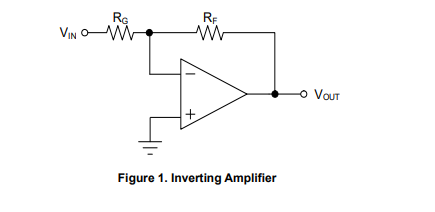
自穩零放大器:高增益傳感器信號放大器的理想選擇
許多傳感器信號放大器處理極小輸入信號的調理。它們的高信號增益要求信號路徑具有極低的失調電壓、隨時間和溫度變化的低失調電壓漂移以及高增益精度。為了用標準線性元件滿足這些要求,需要系統級自動校準和多級放大器。然而,這使得硬件和軟件設計變得復雜,增加了設計成本,并且減慢了新產品的上市時間。
2025-02-21 14:32:171072
1072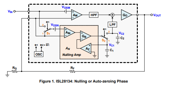
臺階儀精準測量薄膜工藝中的膜厚:制備薄膜理想臺階提高膜厚測量的準確性
固態薄膜因獨特的物理化學性質與功能在諸多領域受重視,其厚度作為關鍵工藝參數,準確測量對真空鍍膜工藝控制意義重大,臺階儀法因其能同時測量膜厚與表面粗糙度而被廣泛應用于航空航天、半導體等領域。費曼儀器
2025-09-05 18:03:23632
632
- 設計技術
- 可編程邏輯
- 電源/新能源
- MEMS/傳感技術
- 測量儀表
- 嵌入式技術
- 制造/封裝
- 模擬技術
- RF/無線
- 接口/總線/驅動
- 處理器/DSP
- EDA/IC設計
- 存儲技術
- 光電顯示
- EMC/EMI設計
- 連接器
- 行業應用
- LEDs
- 汽車電子
- 音視頻及家電
- 通信網絡
- 醫療電子
- 人工智能
- 虛擬現實
- 可穿戴設備
- 機器人
- 安全設備/系統
- 軍用/航空電子
- 移動通信
- 工業控制
- 便攜設備
- 觸控感測
- 物聯網
- 智能電網
- 區塊鏈
- 新科技
- 聯系我們
- 廣告合作
- 王婉珠:wangwanzhu@elecfans.com
- 內容合作
- 張迎輝:mikezhang@elecfans.com
-
關注我們的微信

-
下載發燒友APP

-
電子發燒友觀察

版權所有 ? 湖南華秋數字科技有限公司
長沙市望城經濟技術開發區航空路6號手機智能終端產業園2號廠房3層(0731-88081133)
電子發燒友 (電路圖) 湘公網安備43011202000918 工商網監
湘ICP備2023018690號-1
工商網監
湘ICP備2023018690號-1
評論