顧名思義,output_delay就是指輸出端口的數據相對于參數時鐘邊沿的延時�。
2022-09-26 10:07:10 4831
4831 [ IQmath_fpu32.lib (IQmathTablesRam) ]出現警告 no matching section�����,是不是因為這個警告造成_IQsin()沒有正確執行呢���。希望知道的可以幫我解答下這個問題
2018-08-27 10:25:31
Designing Control Loops for Linear and Switching Power Supplies全英文版����,超清晰,英文原版書籍�����。
2016-05-12 16:34:38
Designing High-Performance Video Systems with the AXI InterconnectHigh-performance video systems
2012-01-26 18:57:03
Designing RF, Analog and Digital on PCB A Unified Systems Approach 設計射頻����,模擬和數字電路板的統一的系統方法
2009-10-10 12:19:49
Designing Safe VHDL State Machines with Synplify
2012-08-13 17:54:58
AVNET - AES-FMC-NETW1-G - Add-On Board, Network Module, For UltraZed FMC Carrier Card, 2 x Ethernet Ports
2024-06-21 02:03:00
ARM System Developers Guide - Designing and Optimizing System Software 體系
2015-04-23 10:22:46
C4_OUTPUT - I/O Modules - Crydom Inc.,
2022-11-04 17:22:44
Impedance Matching Techniques for VLSI PackagingWhy is packaging limiting performance??Inductive
2008-09-10 14:17:54
M_OUTPUT - I/O Modules - Crydom Inc.,
2022-11-04 17:22:44
) are the outstanding features at low current IC=7mA(@VCC=2V). Consider while designing, the device shows potential
2009-05-12 14:00:34
為什么Smith Chart Utility 對話框中點擊Build ADS Circuit 的時候,之前在Smith Chart Matching Network對話框設Zg=30+j*20的阻抗�����,在運行之后就變成了30-j*20了�?
2018-04-20 20:09:44
THS6212的datasheet里面只看到有關于偏置電流的描述���,Inverting input bias current matching能否理解位輸入失調電流?不是話應該怎樣理解�����?
另外
2024-08-09 06:48:49
求audio output express VI ��,自己的labview 找不到
2017-03-26 12:34:19
如圖所示,filter output和filterless output接口有什么區別啊��。����。
2014-08-11 15:21:18
本帖最后由 ye斌 于 2017-8-1 17:07 編輯
在使用視覺助手生成的VI程序,color Matching(顏色匹配)這個空間只能是當時在視覺助手里指定的顏色嗎����?能不能修改��?控件上都沒有選擇路徑的端口���。大神們����,幫幫忙�����,一直要苦惱著....
2017-08-01 17:05:55
Dear Friends, I am designing matching networks at 2.45 GHz. I am using ADS software. I want
2019-07-22 13:40:49
如何做到這一點���,請告訴我。提前致謝�����。 :) 以上來自于谷歌翻譯 以下為原文Hi all, I am designing the conjugate matching circuit for my
2019-07-11 14:15:44
debug\igpio_led_output.out: Error: L6406E: No space in execution regions with .ANY selector
2022-01-12 07:30:16
大家好,你們好:
好吧�,剛才有這個疑惑,但是仔細看了看,明白怎么回事了�����,寫出來分享一下����。
我在閱讀AD8007的datasheet時,想查看AD8007的輸出電壓范圍,也就是Output
2023-11-20 08:14:25
: No space in execution regions with .ANY selector matching board.o(.bss.rt_heap).
.\\\\Output\\\\Debug
2023-09-03 09:42:46
singlecrystal. The MAX7058 has internal tuning capacitors atthe output of the power amplifier that can be programmedfor matching to t
2008-04-25 23:29:02 21
21 The biascurrent and output-matching network for the two-stage PA have been optimized to nominally deliver +18.5dBmwhile consuming 2
2008-08-11 08:47:3014 Impedance Matching Techniques for VLSI Packaging
Problem Statement•Reflections from
2008-09-10 14:16:4113 Designing with 1.5-V Devices
The Cyclone® FPGA family provides the best solution
2009-05-14 10:46:0315 Designing a 33MHz, 32-Bit PCI Target Using ispMACH Devices
The evolution of digital systems over
2009-05-14 11:02:3421 Designing a High Performance SDRAM Controller Using ispMACH Devices
Synchronous DRAMs have become
2009-05-14 11:03:4228 features include on- chip matching and DC blocking on the RF input and output ports. The HFA3424 is packaged in an 8 pin SOIC (Figure 2) whic
2009-06-02 11:07:5318 , such as matching the inputline impedance, signal amplification, signal switching, anddriving the output line, without degrading or adding
2009-06-05 14:26:1619 Designing a 33MHz, 32-Bit PCI Target Using ispMACH Devices
The evolution of digital systems over
2009-06-14 08:47:1960 Designing a High Performance SDRAM Controller Using ispMACH Devices
Synchronous DRAMs have become
2009-06-14 08:55:3124 1.6W Dual Output Flyback Converter using LNK304P:This document is an engineering prototype report
2009-06-28 22:38:4017 output voltages without the needfor a transformer. Typical applications include metering power supplies,where a 3.3 V supply is r
2009-06-28 22:40:2413 48W 2 Output Power Supply using TOP246Y:This document is an engineering report describing a
2009-07-01 00:20:3532 Designing Boards with Atmel AT89C51, AT89C52, AT89C1051, and AT89C2051 for Writing Flash
2009-09-18 09:30:2625 output impedance.Differential current outputs are provided to support singleendedor differential applications. Matching between
2009-09-21 10:04:2011 differential resistance ranging from 5 Ω to 50 Ω. The active back-termination technique provides excellent matching with the output trans
2009-09-23 09:04:1026 differential resistance ranging from 35 Ω to 140 Ω. The active back-termination technique provides excellent matching with the output transmissio
2009-09-23 09:07:2313 with a total output currentof 100mA. Regulated high side internal current sources deliverexcellent current and brightness matching
2009-09-30 09:47:4910 Designing auto power systems with ultracapacitors:Over the last decade, advances in materials
2009-10-01 18:42:2312 平衡的疊層設計(Designing Balanced Printed Circuit Boards):Designers can be tempted to design printed
2009-10-16 00:09:410 Designing a single-stage filter is straightforward. The inductoris selected to give about 20
2009-10-17 10:00:0424 Designing the Power Train of a 200W Power Supply with PFC:Design Issues•System
2009-11-26 11:08:244 This document is an engineering report describing a prototype 2 output universal inputpower supply
2010-01-07 09:22:1118 Voltage-Output DAC
GENERAL DESCRIPTIONThe AD5532 is a 32-channel voltage-output 14-bit DAC withan
2010-04-07 10:23:4617 NCP5623 Triple Output I2C Controlled RGB LED Driver
The NCP5623 mixed analog circuit is a triple
2010-04-19 14:10:0832 Outline• Selecting the right POL Module– T-LynxTM and Naos RaptorTM series• Designing
2010-06-30 19:34:4316 Basic ConceptR26; Outputs can be positive or negative depending on which side ofthe output (top or bottom) is grounded.
�
2010-07-30 10:14:5011 The TLV4120 single supply operational differential amplifier provides a differential output current
2010-09-17 01:17:3411 The amplifier incorporates internal impedance matching to 50 Ω. The part mounted on the standard EVM achieves greater than 15-dB input and output
2010-09-27 19:17:325 WLEDs. Each current output can be individually programmed through external resistors. There is dedicated selection pin for each output, so
2010-10-02 00:51:5011 (PG) function respectively. These devices are capable of supplying 150 mA of output current with a dropout of 115 mV (TPS77133, TPS77233)
2010-10-17 23:47:256 (PG) function respectively. These devices are capable of supplying 150 mA of output current with a dropout of 115 mV (TPS77133, TPS77233)
2010-10-17 23:49:4312 (PG) function respectively. These devices are capable of supplying 150 mA of output current with a dropout of 115 mV (TPS77133, TPS77233)
2010-10-17 23:54:518 (PG) function respectively. These devices are capable of supplying 150 mA of output current with a dropout of 115 mV (TPS77133, TPS77233)
2010-10-18 00:29:0314 (PG) function respectively. These devices are capable of supplying 150 mA of output current with a dropout of 115 mV (TPS77133, TPS77233)
2010-10-18 00:34:3712 (PG) function respectively. These devices are capable of supplying 150 mA of output current with a dropout of 115 mV (TPS77133, TPS77233)
2010-10-18 20:41:554 The PTB4850x power modules are a dual-output isolated DC/DC converter, designed to provide
2010-11-12 14:37:248 The PTB4850x power modules are a dual-output isolated DC/DC converter, designed to provide
2010-11-12 14:44:5410 The PTB4850x power modules are a dual-output isolated DC/DC converter, designed to provide
2010-11-12 14:46:3813 ABSTRACTWhen designing with switching regulators, application requirements determine howmuch input
2010-11-16 17:05:4536 Dual, Voltage-Output DAC Consumes Miniscule Power
The dual, voltage-output DACs shown
2008-11-24 10:19:581165 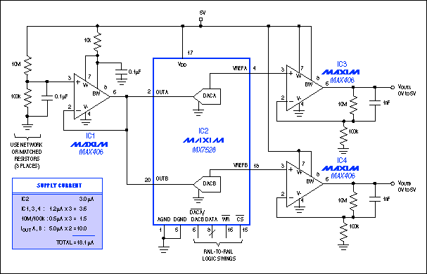
Designing the DS2726 to Protect Li+ Batteries During a Reverse Charger Event
Abstract:
2008-12-18 10:05:47987 
Designing the DS2726 to Protect Li+ Batteries During a Reverse Charger Event
Abstract
2008-12-20 12:46:351386 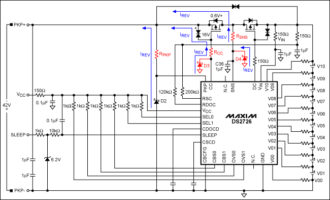
MAX15034 Dual-Output, Synchronous Step-Down Controller Provides Two 25A Outputs or a Single 50A
2009-01-11 11:38:241155 
MAX15023 Dual-Output, Synchronous DC-DC Controller with Wide Operating Range Delivers Up to 25A
2009-01-28 15:00:301271 Abstract: When designing microprocessor cards and memory subsystems cards for backplane-based
2009-04-24 09:53:221064 
Abstract: The digital, pulse-width-modulation (PWM) output available from many microprocessors
2009-04-26 16:50:551001 
Abstract: This application note examines the effect of the output filter on audio Class D amplifier
2009-05-06 11:59:231809 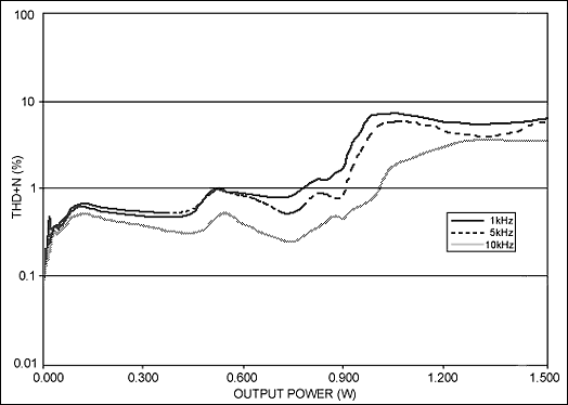
設計基于LED的視頻顯示板 Designing an LED-Based Video-Display Board
Abstract: Currently, all of the top LED
2009-07-18 11:12:251981 Adjusting the output voltages of the MAX8660/MAX8661
Abstract: The MAX8660/MAX8661 PMICs (power management ICs) have the most common output v
2009-12-26 00:02:26851 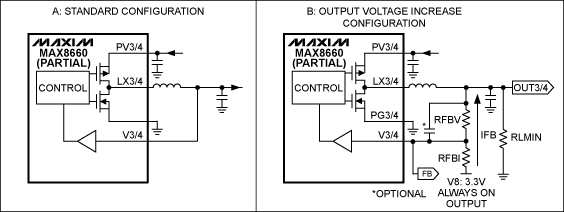
in industrialprocess control equipment, analytical and scientificinstruments and automatic test equipment. In the past,designing a universal output modu
2012-02-03 15:55:2756 東芝光耦 MOSFET Output���,Photorelays (MOSFET Output)
2012-03-16 13:44:59769 
電子發燒友網站提供《Matching阻抗匹配計算軟件(dos).exe》資料免費下載
2014-06-12 16:32:1412 DC TO DC INVERTER 詳細介紹 歡迎免費下載
2016-01-11 14:48:3325 Designing with a New Super Fast Dual Norton Amplifier
2017-03-24 15:48:300 Designing High Speed Active Filters
2017-03-24 15:32:380 不符,并影響硅片上的性能�����。相比之下����,采用Calibre@ Pattern MatcHing方法更為合理,其代碼可輕松編寫到SVRF中�����,驗證器件版圖并通過與圖形交互輸出不匹配的形狀��。
2018-03-05 15:16:3816 為設計增加線末端延長量是一種提高良率和可靠性的簡單方法���。但是��,將這些強化技術編碼到物理驗證規則集中則需要專家級的代碼編寫能力,并會加重未來改進規則集的支持負擔。使用Calibre Pattern Matching功能以圖形方式識別合規區域可降低所需的編碼專業水平�,并可在增加額外標準時輕松更新���。
2018-03-06 16:16:326 , GPIO.OUT)2、設置某個輸出針腳狀態為高電平:12345GPIO.output(12, GPIO.HIGH)?# 或者GPIO.output(12,?1)?# 或者GPIO.output
2019-04-02 14:42:371186 電子發燒友網為你提供ADI(ti)SCP-OUTPUT-EVALZ相關產品參數���、數據手冊,更有SCP-OUTPUT-EVALZ的引腳圖�����、接線圖�����、封裝手冊���、中文資料�、英文資料�����,SCP-OUTPUT-EVALZ真值表��,SCP-OUTPUT-EVALZ管腳等資料�����,希望可以幫助到廣大的電子工程師們。
2021-07-09 21:00:04
電子發燒友網站提供《N7DCC Matching 1.8到50MHz頻段的天線設備.zip》資料免費下載
2022-07-22 15:18:132 在Output Job中選擇[Project Physical Documents],將會顯示編譯后的原理圖圖紙�����,其中包含圖紙上不同的變量元素����。
2022-09-08 11:20:461514 編譯時出現warning:no matching section
-l rts2800_XXXXX.lib(.text)的解決方案
2022-10-31 08:23:310 相對于電感、電容構成的阻抗匹配網絡而言,Matching PAD具有更平坦的幅頻響應、更好的阻抗匹配效果,廣泛應用于廣播���、電視信號測試系統���。
2023-06-12 10:25:561664 
電子發燒友網為你提供ADI(ADI)MAX77720: Wide Output-Voltage Range, Dual- Polarity PMIC Data Sheet相關產品參數�、數據手冊,更有
2023-10-12 18:40:53

電子發燒友網為你提供ADI(ADI)Evaluation Kit for MAXM17572 in 5V Output Application Data Sheet相關產品參數�、數據手冊��,更有
2023-10-12 18:50:51
電子發燒友網為你提供ADI(ADI)HMC955: 32 Gbps, 1:2 Demux with Programmable Output Voltage Data Sheet相關產品參數、數據手冊
2023-10-13 18:32:14
電子發燒友網為你提供ADI(ADI)HMC940: 13 Gbps, 1:4 Fanout Buffer w/ Programmable Output Voltage Data Sheet相關產品
2023-10-13 18:33:07
電子發燒友網為你提供ADI(ADI)MAX14906: Quad-Channel Industrial Digital Output, Digital Input Data Sheet相關產品參數
2023-10-13 18:44:47
電子發燒友網為你提供ADI(ADI)MAX25540: Automotive 4-Output Display Power Solution Data Sheet相關產品參數��、數據手冊��,更有
2023-10-13 19:20:16
電子發燒友網為你提供ADI(ADI)MAX25250: Four Output Mini PMIC for Camera Applications Data Sheet相關產品參數�����、數據手冊,更有
2023-10-17 18:51:43
在Verilog中�����,input和output用于定義模塊的輸入和輸出端口����。它們是用于通信的關鍵元素,定義了模塊與其它模塊之間的數據傳輸接口�。通過input和output端口����,模塊之間可以互相傳遞數據
2024-02-23 10:29:275266 功放(Power Amplifier)的output接口是指功放器件輸出信號的端口���,用于連接音箱或揚聲器等音頻設備����。功放的output接口具有以下作用: 功率輸出:功放的主要功能是將低功率的音頻
2024-02-23 10:32:0412038 功放機是音頻系統中不可或缺的組成部分��。作為信號處理與擴大音頻信號的設備�,功放機的OUTPUT接口在連接音頻信號與外部設備之間起到了橋梁的作用���。本文將詳細介紹功放機的OUTPUT接口的類型��、功能
2024-02-23 10:34:0024870 在計算機科學領域��,輸出被認為是一個程序或系統產生的結果。output1和output2是兩個常見的輸出標識�����,它們在不同的上下文中具有不同的含義和用途���。 output1的定義和用途 output1通常
2024-02-23 13:45:034149
 電子發燒友App


 工商網監
工商網監
評論