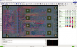
 PCB設計中怎樣消除反射噪聲

什么是反射噪聲?反射噪聲會對你的PCB性能產生什么影響?如何能夠做到盡可能低的反射噪聲?
這是網站“Allaboutcircuits()”上的一篇英文文章,在此分享給大家,供有志于用英語閱讀技術文章的朋友參考。
What Is Reflection Noise?
Whenever we send a signal from one digital integrated circuit to another on our PCBs, we change the state of a signal line. That change in state and the accompanying changes in the electromagnetic fields can be described as a wave as it moves through the circuit. Waves are phenomena that transfer energy from one location to another, with conductors guiding the path of propagation.

This is an artistic impression of magnetic energy surrounding a wire as the potential of the wire changes.
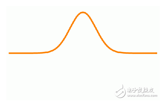
Reflection noise results when an electromagnetic wave encounters a boundary from one medium to the next. When the wave meets the boundary, part of the energy is transmitted as signal and part of it is reflected.
This animation illustrates that, when waves travel from one medium to another, not all energy is transmitted—a portion of the energy is reflected back to its source.
For electrical engineers, the medium where this boundary occurs is usually described in terms of its electrical impedance; that is, the boundary is where impedance changes.
Impedance is composed of resistive and reactive elements. Resistors dissipate a circuit’s energy as heat. The recoverable energy in a circuit exists in the electromagnetic fields that permeate and surround conductors, inductors, and capacitors.
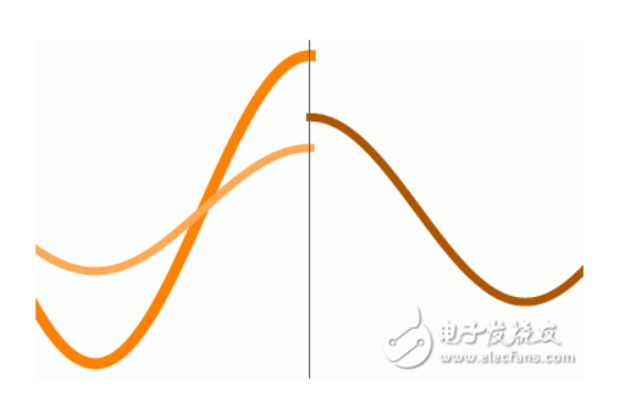
Whenever the impedance changes in a circuit, some amount of reflection will occur. The reflected wave will travel back to the next boundary (the location where there is a change in impedance) and reflect again.
This 1D wave illustration shows a wave pulse reflected between two points. The energy is attenuated over time/distance.
The process will continue indefinitely until the energy is absorbed by the circuit or dissipated into the environment.
Why Is Reflection Noise a Problem?
For signal lines, there will be reflection points at your driver and receiver. The job of the engineer is to minimize the amount of reflected signal and maximize the amount of transmitted signal through impedance matching.
If that is not possible, the additional energy will need to be dissipated before it accumulates and drowns out a signal with noise.
If the energy of the reflected pulse does not dissipate before the next pulse is generated, the energy will accumulate and add in a phenomenon called superposition. Fortunately, signals attenuate as they pass through resistive elements. So a simple series resistor will eliminate most ringing.
Assessing Noise in Digital Signals
Fourier’s theorem teaches that any wave or wave-pulse can be decomposed into a series of sine and/or cosine waves. If you'd like more insight into this concept, I recommend this video on the harmonic analyzer with Bill Hammack of the University of Illinois.
If you have a sufficiently small rise/fall time, a single pulse can hold in it dozens of small-amplitude waves.
In the image below, you can see an undamped digital signal switching logic states from low to high.
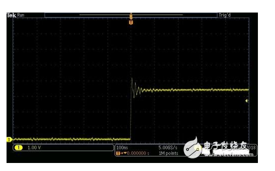
An undamped digital signal (yellow, channel 1) captured on a TI Lightcrafter as it switches logic states from low to high.
Now check out the image below, where the left-hand image shows a composite wave pulse created through the successive superposition of decreasing amplitude odd-harmonics of the original wave. For signals of practical interest, we can decompose the waveform into a series of sine waves.
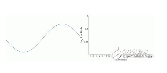
As the above figures show, a real digital signal has a large bandwidth and any portion of that energy might create a resonance in your circuit. This is in contrast to RF signals that have very narrow bandwidth with easy to calculate resonances.
If you do manage to create standing waves, you will create enormous sources of noise that can overwhelm any signal line in the vicinity.
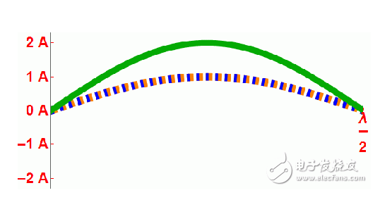
This gif shows that a wave (orange) reflected at a particular wavelength can combine with its reflection (blue) to create a high amplitude standing wave (green). This phenomenon will happen at odd-integer multiples of ? wavelength, where the wavelength is twice the length of your trace.
How to Reduce Reflection Noise
There are several methods you can use to manage reflection noise in your design. Here's an overview of some of the techniques at your disposal.
-
pcb
+關注
關注
4415文章
23933瀏覽量
425710 -
華強pcb線路板打樣
+關注
關注
5文章
14629瀏覽量
44701
發布評論請先 登錄
淺談晶振在PCB設計中的要點

PCB設計與打樣的6大核心區別,看完少走3個月彎路!
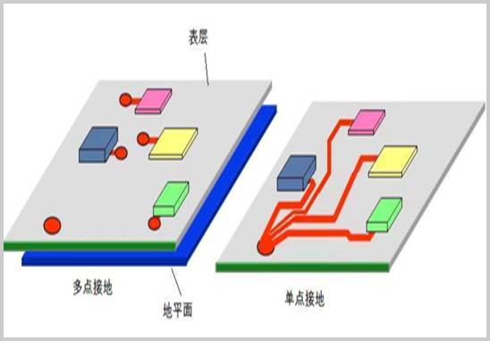
PCB設計中單點接地與多點接地的區別與設計要點
深度解讀PCB設計布局準則
上海圖元軟件國產高端PCB設計解決方案
PCB設計與工藝規范

PCB設計,輕松歸檔,效率倍增!

原理圖和PCB設計中的常見錯誤
高頻PCB設計中出現的干擾分析及對策
DDR模塊的PCB設計要點
解決噪聲問題試試從PCB布局布線入手
Altium Designer中PCB設計規則設置

PCB設計中容易遇到的問題
提升PCB設計效率的秘訣


 工商網監
工商網監
評論