") 【ALINX 教程】FPGA Multiboot 功能實(shí)現(xiàn)——基于 ALINX Artix US+ AXAU25 開發(fā)板
【ALINX 教程】FPGA Multiboot 功能實(shí)現(xiàn)——基于 ALINX Artix US+ AXAU25 開發(fā)板

教程目的
本教程介紹如何在ALINX Artix US+ AXAU25 FPGA開發(fā)板上,通過Multiboot實(shí)現(xiàn)多個(gè) bitstream 的存儲(chǔ)與動(dòng)態(tài)切換,并在配置失敗時(shí)自動(dòng)回退至安全鏡像(Golden Image)。
適用對(duì)象
已掌握 FPGA 基礎(chǔ)開發(fā)(會(huì)寫Verilog、會(huì)生成bitstream)
熟悉 Vivado 工程流程
對(duì) FPGA 配置機(jī)制尚不深入,希望進(jìn)入系統(tǒng)級(jí)設(shè)計(jì)階段的學(xué)習(xí)者
Multiboot 功能概述
在基礎(chǔ)實(shí)驗(yàn)中,F(xiàn)PGA 通常通過 JTAG 下載 bitstream,這種方式掉電后配置就丟失,亦無法實(shí)現(xiàn)遠(yuǎn)程升級(jí)。Multiboot 通過將多個(gè)配置鏡像存儲(chǔ)在外部 Flash 中,使 FPGA 能夠在上電或運(yùn)行過程中,從不同地址加載不同的 bitstream,并在異常情況下自動(dòng)回退,保證系統(tǒng)可恢復(fù)。
Golden Image:固定存放在 Flash 的 0 地址,功能最小、穩(wěn)定可靠,負(fù)責(zé)系統(tǒng)初始化與升級(jí)控制。
Multiboot Image:存放在 Flash 的其他地址,承載具體業(yè)務(wù)邏輯,可被升級(jí)或替換。
下圖展示了 FPGA Multiboot 機(jī)制的整體配置與啟動(dòng)流程:FPGA 上電后默認(rèn)從 Flash 0 地址加載 Golden Image,在滿足觸發(fā)條件后,通過 MultiBoot 機(jī)制嘗試從 Upper Address 加載 MultiBoot Image。當(dāng)配置成功時(shí)運(yùn)行 MultiBoot Image;若配置失敗,則觸發(fā) Fallback 機(jī)制,自動(dòng)回退并重新加載 Golden Image,以保證系統(tǒng)仍可正常運(yùn)行。
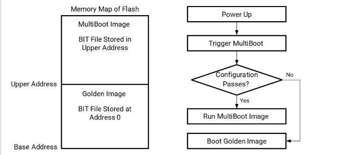 (Multiboot 運(yùn)行流程示意圖)
Multiboot 實(shí)現(xiàn)方式


AMD FPGA 支持兩種 Multiboot 實(shí)現(xiàn)方式,一種是在生成 bitstream 時(shí)嵌入 IPROG,另一種是通過用戶邏輯控制 ICAP 接口觸發(fā)重配置,本教程采用ICAP+IPROG的動(dòng)態(tài)方式,可在 FPGA 運(yùn)行過程中靈活控制重配置行為,更符合實(shí)際工程需求。
Multiboot 功能實(shí)現(xiàn)
使用硬件
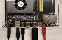
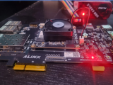
開發(fā)板:ALINX AXAU25
FPGA:AMD Artix UltraScale+(XCAU25P)
啟動(dòng)方式:SPI Flash(x4 模式)
該平臺(tái)原生支持 MultiBoot 與 Fallback。
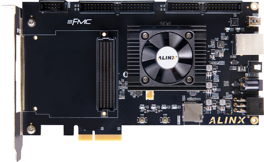
(ALINX基于Artix UltraScale+ FPGA開發(fā)板AXAU25)
工程實(shí)現(xiàn)
Golden Image 設(shè)計(jì)
//===========================================================================
// Module name: led_test.v
//===========================================================================
`timescale 1ns / 1ps

module multiboot_top
(
input  sys_clk_p,      // Difference system clock 200Mhz input on board
input  sys_clk_n,
output reg  led            // LED,use for control the LED signal on board

 );

//define the time counter
reg [31:0]   timer;
wire [31:0]   WBSTAR;


//===========================================================================
//Differentia system clock to single end clock
//===========================================================================
wire        rst_n;
wire        sys_clk_buf;
wire        sys_clk;
wire        switch;
wire        switch_d0;
wire        switch_d1;
 IBUFGDS u_ibufg_sys_clk   //????????????????
     (
      .I  (sys_clk_p),
      .IB (sys_clk_n),
      .O  (sys_clk_buf  )
      );

  clk_wiz_0 syspll
   (
    // Clock out ports
    .clk_out1(sys_clk),     // output clk_out1
    // Status and control signals
    .locked(rst_n),       // output locked
   // Clock in ports
    .clk_in1(sys_clk_buf));


vio_0 uu (
  .clk(sys_clk),                // input wire clk
  .probe_out0(switch),  // output wire [0 : 0] probe_out0
  .probe_out1(WBSTAR)  // output wire [31 : 0] probe_out1
);
//===========================================================================

//===========================================================================
  always @(posedge sys_clk)
    begin
      if (~rst_n)
          timer <= 32'd0;                     // when the reset signal valid,time counter clearing
      else if (timer == 32'd99_999_999)    //1 seconds count(200M-1=199999999) ?????200Mhz??????5ns??????0-199_999_999,??2*10^8??????
          timer <= 32'd0;                       //count done,clearing the time counter
      else
                    timer <= timer + 1'b1;            //timer counter = timer counter + 1????????????????
    end

//===========================================================================
// LED control
//===========================================================================
  always @(posedge sys_clk)
    begin
      if (~rst_n)
          led <= 0;                  //when the reset signal active
      else if (timer == 32'd99_999_999)   //time counter count to 1 sec,LED4 lighten
          led <= ~led;
    end

(* MARK_DEBUG="true" *)reg  ce ;
(* MARK_DEBUG="true" *)reg  write ;
(* MARK_DEBUG="true" *)reg [31:0]  icap_in ;
(* MARK_DEBUG="true" *)wire [31:0]  icap_in_wire ;

   ICAPE3 #(
      .DEVICE_ID(32'h04A64093),     // Specifies the pre-programmed Device ID value to be used for simulation
                                    // purposes.
      .ICAP_AUTO_SWITCH("DISABLE"), // Enable switch ICAP using sync word.
      .SIM_CFG_FILE_NAME("NONE")    // Specifies the Raw Bitstream (RBT) file to be parsed by the simulation
                                    // model.
   )
   ICAPE3_inst (
      .AVAIL(),     // 1-bit output: Availability status of ICAP.
      .O(O),             // 32-bit output: Configuration data output bus.
      .PRDONE(),   // 1-bit output: Indicates completion of Partial Reconfiguration.
      .PRERROR(), // 1-bit output: Indicates error during Partial Reconfiguration.
      .CLK(sys_clk),         // 1-bit input: Clock input.
      .CSIB(ce),       // 1-bit input: Active-Low ICAP enable.
      .I(icap_in_wire),             // 32-bit input: Configuration data input bus.
      .RDWRB(write)      // 1-bit input: Read/Write Select input.
   );

localparam        [31:0]        DUMMY_WORD                = 32'hFFFFFFFF;
localparam        [31:0]        SYNC_WORD            = 32'hAA995566;
localparam        [31:0]        TYPE1_NOOP                = 32'h20000000;
localparam        [31:0]        TYPE1_WBSTAR        = 32'h30020001;
localparam        [31:0]        TYPE1_CMD                  = 32'h30008001;
localparam        [31:0]        IPROG_CMD                  = 32'h0000000F;

// localparam  [31:0]  WBSTAR        = 32'h04000000;

(* MARK_DEBUG="true" *)reg [3:0]  state ;


assign icap_in_wire = {icap_in[3*8+0],icap_in[3*8+1],icap_in[3*8+2],icap_in[3*8+3],icap_in[3*8+4],icap_in[3*8+5],icap_in[3*8+6],icap_in[3*8+7],
                      icap_in[2*8+0],icap_in[2*8+1],icap_in[2*8+2],icap_in[2*8+3],icap_in[2*8+4],icap_in[2*8+5],icap_in[2*8+6],icap_in[2*8+7],
                      icap_in[1*8+0],icap_in[1*8+1],icap_in[1*8+2],icap_in[1*8+3],icap_in[1*8+4],icap_in[1*8+5],icap_in[1*8+6],icap_in[1*8+7],
                      icap_in[0*8+0],icap_in[0*8+1],icap_in[0*8+2],icap_in[0*8+3],icap_in[0*8+4],icap_in[0*8+5],icap_in[0*8+6],icap_in[0*8+7]};


always @(posedge sys_clk ) begin
  if (~rst_n)  begin
    state <= 0 ;
    ce <= 0 ;
    write <= 0 ;
    icap_in <= DUMMY_WORD ;
  end
  else begin
    case (state)
      0: begin
        if (switch) begin
          state <= 1 ;
          icap_in <= DUMMY_WORD ;   //Dummy word
          write <= 0 ;
          ce <= 0 ;
        end
      end
      1: begin
        state <= 2 ;
        icap_in <= SYNC_WORD ;   //sync word
      end
      2: begin
        state <= 3 ;
        icap_in <= TYPE1_NOOP ;   //Type 1 NOOP
      end
      3: begin
        state <= 4 ;
        icap_in <= TYPE1_WBSTAR ;   //Type 1 Write 1 words to WBSTAR
      end
      4: begin
        state <= 5 ;
        icap_in <= WBSTAR ;   //Warm boot start address (Load the desired address)
      end
      5: begin
        state <= 6 ;
        icap_in <= TYPE1_CMD ;   //Type 1 Write 1 words to CMD
      end
      6: begin
        state <= 7 ;
        icap_in <= IPROG_CMD ;   //IPROG command
      end
      7: begin
        state <= 8 ;
        icap_in <= TYPE1_NOOP ;   //Type 1 NOOP
      end
      8: begin
        state <= 8 ;
        write <= 1 ;
        ce <= 1 ;
        icap_in <= 0 ;
      end
      default: begin
        state <= 0 ;
        ce <= 1 ;
        write <= 1 ;
        icap_in <= DUMMY_WORD ;
      end
    endcase
  end
end


endmodule

XDC 約束
############## clock define##################
create_clock -period 5.000 [get_ports sys_clk_p]
set_property PACKAGE_PIN T24 [get_ports sys_clk_p]
set_property PACKAGE_PIN U24 [get_ports sys_clk_n]
set_property IOSTANDARD DIFF_SSTL18_I [get_ports sys_clk_n]


##############LED define##################
set_property PACKAGE_PIN W21 [get_ports led]
set_property IOSTANDARD LVCMOS18 [get_ports led]


set_property CONFIG_MODE SPIx4 [current_design]
set_property BITSTREAM.CONFIG.CONFIGRATE 85.0 [current_design]
set_property BITSTREAM.CONFIG.SPI_32BIT_ADDR YES [current_design]
set_property BITSTREAM.CONFIG.SPI_BUSWIDTH 4 [current_design]
set_property BITSTREAM.CONFIG.SPI_FALL_EDGE YES [current_design]
set_property BITSTREAM.CONFIG.CONFIGFALLBACK ENABLE [current_design]

set_property BITSTREAM.GENERAL.COMPRESS TRUE [current_design]
Multiboot Image 設(shè)計(jì)
`timescale 1ns / 1ps
module multiboot(
//Differential system clock
    input sys_clk_p,
    input sys_clk_n,
    input rst_n,
(* MARK_DEBUG="true" *)    output reg [1:0] led
    );
(* MARK_DEBUG="true" *)reg[31:0] timer_cnt;
wire sys_clk ;

IBUFDS IBUFDS_inst (
      .O(sys_clk),   // 1-bit output: Buffer output
      .I(sys_clk_p),   // 1-bit input: Diff_p buffer input (connect directly to top-level port)
      .IB(sys_clk_n)  // 1-bit input: Diff_n buffer input (connect directly to top-level port)
   );

always@(posedge sys_clk)
begin
    if (!rst_n)
    begin
      led <= 2'b0 ;
    end
    else if(timer_cnt <= 32'd100_000_000)
    begin
        led <= 2'b10;
    end
    else begin
         led <= 2'b01;
    end
end

always@(posedge sys_clk)begin
    if(!rst_n)begin
        timer_cnt <= 32'b0;
    end
    else if(timer_cnt >= 32'd199_999_999)   //1 second counter, 200M-1=199_999_999
    begin
        timer_cnt <= 32'd0;
    end
    else begin
        timer_cnt <= timer_cnt + 1;
    end
end


endmodule
xdc約束
set_property PACKAGE_PIN T24 [get_ports sys_clk_p]
set_property PACKAGE_PIN N26 [get_ports rst_n]
set_property PACKAGE_PIN W21 [get_ports led]
set_property IOSTANDARD LVCMOS18 [get_ports {led[1]}]
set_property IOSTANDARD LVCMOS18 [get_ports {led[0]}]
set_property IOSTANDARD LVCMOS18 [get_ports rst_n]
set_property IOSTANDARD DIFF_SSTL18_I [get_ports sys_clk_p]

set_property PACKAGE_PIN AC16 [get_ports {led[0]}]
set_property PACKAGE_PIN W21 [get_ports {led[1]}]

create_clock -period 5.000 -name sys_clk_p -waveform {0.000 2.500} [get_ports sys_clk_p]

set_property BITSTREAM.CONFIG.CONFIGFALLBACK ENABLE [current_design]
set_property BITSTREAM.GENERAL.COMPRESS TRUE [current_design]
set_property BITSTREAM.CONFIG.SPI_BUSWIDTH 4 [current_design]
set_property BITSTREAM.CONFIG.SPI_32BIT_ADDR YES [current_design]
設(shè)備的 ID 是固定按照提供資料查詢相關(guān)操作設(shè)備 ID

下方列表是通過 ICAP 接口進(jìn)行 IPROG 中需要執(zhí)行的命令

通過 Vivado 將需要固化的兩個(gè) bit 文件合成一個(gè)燒寫文件,燒寫完成斷電重新上電即可。

實(shí)驗(yàn)結(jié)果

默認(rèn)加載 Golden Image,LED 1閃爍
通過 VIO 設(shè)置
switch=1,WBSTAR=0x0080_0000(我們?cè)?Flash 中存放的第二個(gè) Multiboot Image 的初始地址),等待一段時(shí)間,LED 1、LED 2 交替閃爍,MultiBoot Image 切換成功。
參考文檔
UltraScale Architecture Configuration User Guide (UG570)
Vivado Design Suite 用戶指南: 編程和調(diào)試 (UG908)
歡迎您聯(lián)系我們,一起交流技術(shù)。
審核編輯 黃宇
-
FPGA
+關(guān)注
關(guān)注
1662文章
22464瀏覽量
637998
發(fā)布評(píng)論請(qǐng)先 登錄
直擊玄鐵RISC-V生態(tài)大會(huì),看ALINX FPGA+RISC-V解決方案
重磅新品亮相國際!ALINX 誠邀您蒞臨 Embedded World 2026

【ALINX選型】AMD Kintex UltraScale+ 系列 FPGA 開發(fā)板速選
FPGA 專業(yè)級(jí)開發(fā)平臺(tái)性價(jià)比之選,ALINX Artix US+ PCle AXAU25
ALINX教程分享_Zynq UltraScale+ MPSoC PYNQ3.1.2移植
ALINX全球區(qū)域服務(wù)網(wǎng)絡(luò)介紹
SCI 期刊驗(yàn)證!蘇黎世大學(xué)使用 ALINX FPGA 開發(fā)板實(shí)現(xiàn)分子動(dòng)力學(xué)模擬新方案
2025 ALINX入門競(jìng)賽類FPGA開發(fā)板選型指南
ALINX 助力希臘 SpaceDot AcubeSAT 衛(wèi)星項(xiàng)目,2026 將入太空
從應(yīng)用場(chǎng)景看國產(chǎn)化FPGA潛力,紫光同創(chuàng)研討會(huì)武漢·北京站回顧

ALINX AMD RFSoC 射頻開發(fā)板選型全攻略!
ALINX AMD RFSoC射頻開發(fā)板選型指南
使用ALINX VD100開發(fā)板實(shí)現(xiàn)圖像處理
ALINX 邀您相聚 2025 慕尼黑上海電子展


 工商網(wǎng)監(jiān)
評(píng)論