 Efinity Interface Designer報錯案例-v2

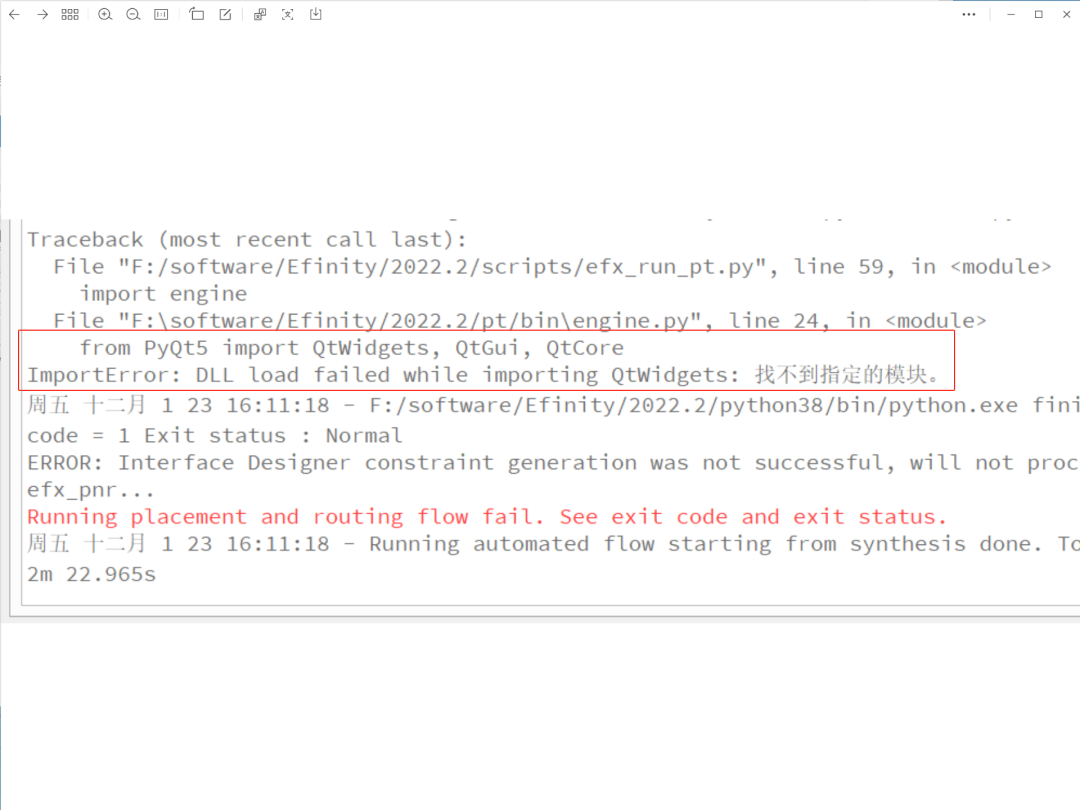
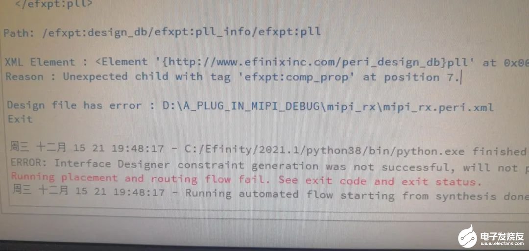
(1)ERROR:Interface Designer constraint generation was not successfull,will not proceed to efx_pnr...

原因:(1)有些客戶使用Win7版本,目前Efinity對Win7的支持不好。建議升級成win10。
(2)殺毒軟件刪除了文件,實際interface生成約束是沒有問題的,客戶pnr的時候就報錯,需要重新安裝軟件。
(3)電腦存在加密系統 。造成的現象是新建工程時interface可以打開,但是生成xxx.peri.xml文件之后再次打開就會報錯。
(2)Interface打不開。
現象:(1)打開interface的時候指示:Efinity Interface Designer finished. Exit code = 1 Exit status : NormalInterface design file exists, check and migrate done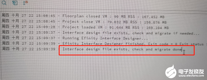 (2)新建工程第一次可以打開interface Designer(3)刪除xxx.peri.xml之后,第一次也可以打開Interface Designer.原因:電腦存在加密
(3) interface打不開打開interface Designer時會報以下錯誤。EfinityIPCatalogfinished.Exit code = 0Exit status:Normal
(2)新建工程第一次可以打開interface Designer(3)刪除xxx.peri.xml之后,第一次也可以打開Interface Designer.原因:電腦存在加密
(3) interface打不開打開interface Designer時會報以下錯誤。EfinityIPCatalogfinished.Exit code = 0Exit status:Normal
編譯過程可能報以下錯誤:
ERROR: Interface Designer constraint generation was not successful, will not processpnr..
(4)repeated,non-bussed pin found in verilog template generation:clk_27m
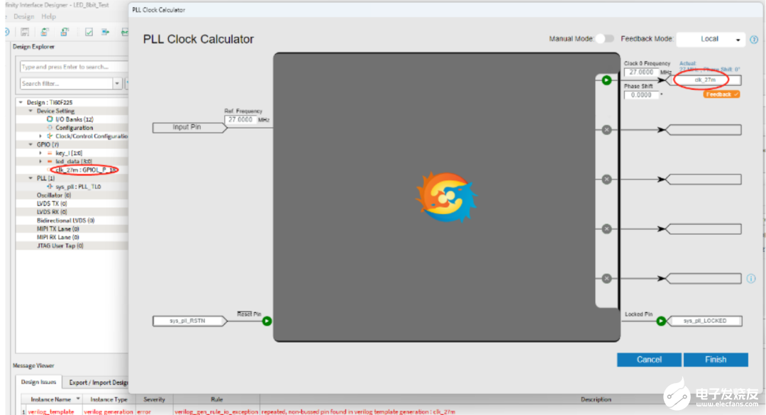
說明:在GPIO處定義了一個clk_27m,在pll的輸出上又定義了一個clk_27m,兩個信號名沖突。
(5)ERROR: Interface Designer constraint generation was not successful, will not processpnr..
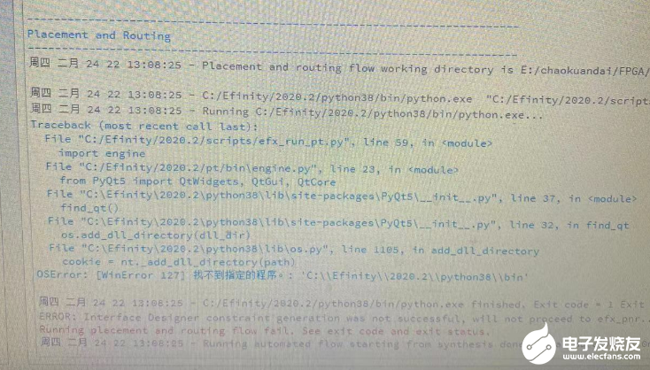
原因:1)一般是軟件有360或者別的殺毒軟件的相關文件刪除了,需要找回文件或者重新安裝軟件。
2)客戶使用Win7版本,目前Efinity對Win7的支持不好。建議升級成win10。
(6)cannot connect to more than 4 different clocks per region on left and right
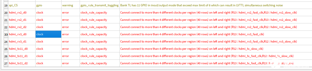
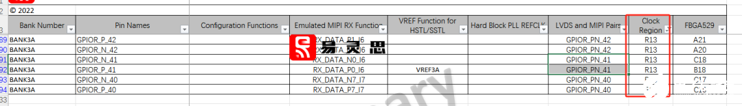
原因是在pinout文件中對應的Clock Region中,不能超過4個時鐘去驅動。
-
也就是GPIOR_PN_42,41,40三組差分對,不能由兩組LVDS來驅動,因為每組LVDS時鐘有lvds_fast_clk和lvds_slow_clk兩個,兩組就會有4個時鐘在Region clock R13區域。
-
結論就是把LVDS差分對放在同一個Clock Region.
(7)Resource name is empty
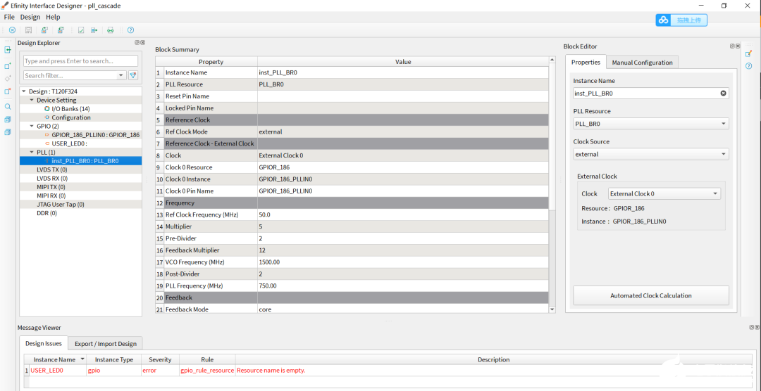
解決方案:Resource是指管腳,這里是指沒有分配管腳。
(8)用新版本軟件打開老版本工程時interface Desinger打不開
發給客戶的peri.xml,客戶打不開有問題,叫他們文本打開peri看看,有些客戶沒有動peri文件,但是內容卻改了
(9) Valid characters are alphanumeric haracters with dash and underscore only
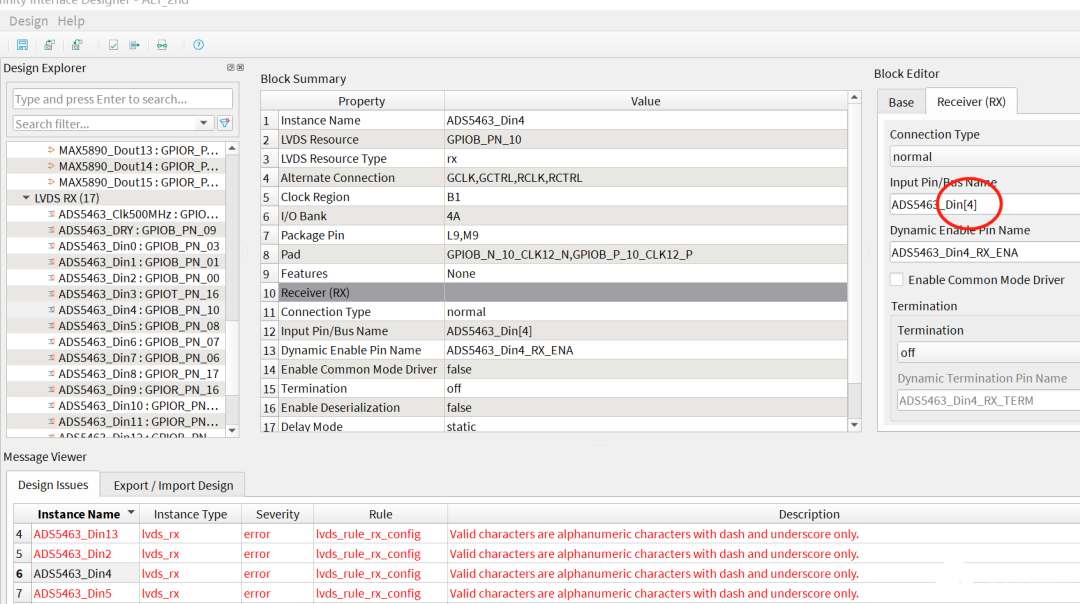
原因:在LVDS添加Block時不能添加bus,所以在Input Pin/Bus Name中命名上不能像總線一樣添加[*]
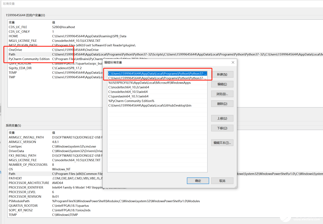
(10)interface Designer打不開定位思路。
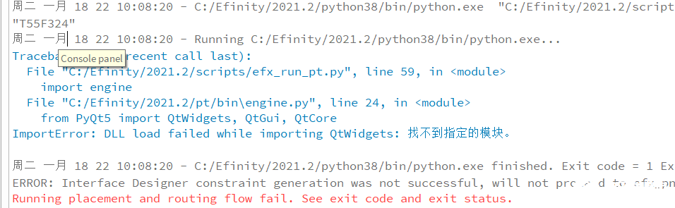
原因:查一下下面幾點:
1. 系統環境路徑設置
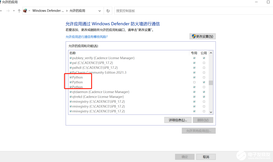
2. python是否在firewall 允許的程序列表里
3. microsoft visual c++2015有安裝嗎?
這個有一個安裝包,在打不開的時候可以安裝
4. java 8有安裝嗎?
(11)燒寫文件無法生成Using source file "D:/customer_Prj/googol/phy_jtag_bridge/work_pnr/spi_flash_loader.lbf"Missing Interface Designer LPF constraint file, no programming file will be generated.Open Interface Designer to createa project.原因:如果在interface Desinger中沒有添加接口是不會生成bit文件的。
(12)These HSIOGPlOmust be placed at least 1 pair away from Mipl lane csi_rxc in order to avoid noise coupling from GPIOto MIPILane: GPIOR_ N_09,GPIOR_P 09
這個是一告警信息,意思是說差分信號要和單端信號之間隔開一組差分對。比如上面的警告,說的是GPIOR_PN_09這個差分對和要單端信號之間隔開一組差分對,也就是GPIOR_PN_08或者GPIOR_PN_10要空著不能接信號。當然如果放一些很低速的信號也是可以的比如復位信號,上電之后一般不再翻轉,或者UART這樣速率比較低的信號。
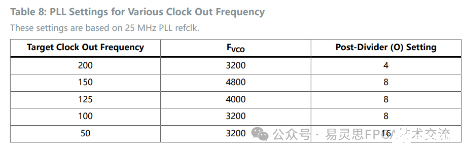
(13)The recommended phase shit step for the Calibration Clock is 45 degrees, Curent: 15.0000 degrees.
在使用hyperram時,對fpll的頻率是有要求的。請具體參考以下格式對PLL的VCO頻率和POST-divider參數進行設置。更詳細的說明可以參考hyperram的datasheet或者本公眾號關于hyperram的介紹。
-
Interface
+關注
關注
0文章
103瀏覽量
39715
發布評論請先 登錄
AA Boost Module V2:便捷的電源解決方案
如何在 VisionFive v2 上使用外部 GPU?
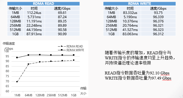
RDMA設計44:RoCE v2原語功能驗證與分析

RDMA設計37:RoCE v2 子系統模型設計
RDMA設計30:RoCE v2 發送模塊2
RDMA設計29:RoCE v2 發送及接收模塊設計2
RDMA設計28:RoCE v2 發送及接收模塊設計
RDMA設計19:RoCE v2 發送及接收模塊設計
uIO-Stick v2 用戶指南:設計、應用與安全要點
Efinity RISC-V IDE入門使用-5
RDMA over RoCE V2設計1:為什么要設計它?
Efinity debuger常見問題總結-v4
在V2板子上部署豆包模型調試指南
HarmonyOS Next V2 @Local 和@Param


 工商網監
工商網監
評論