") 深入解析onsemi NCP81428:高性能熱插拔智能保險絲的卓越之選
深入解析onsemi NCP81428:高性能熱插拔智能保險絲的卓越之選

深入解析onsemi NCP81428:高性能熱插拔智能保險絲的卓越之選
在電子設備的設計中,保護電路免受各種異常狀況的影響至關重要。onsemi的NCP81428作為一款PMBus? 兼容的12 V、50 A可復位在線保險絲,為服務器、數(shù)據(jù)存儲、基站和工業(yè)應用等領域提供了全面的保護解決方案。下面我們就來詳細了解一下這款產品。
文件下載:onsemi NCP81428 PmBus?熱插拔智能保險絲.pdf
產品概述
NCP81428集成了0.65 mΩ NMOS FET、高性能熱插拔控制器和非易失性存儲器(NVM),采用LQFN32封裝。它能夠有效應對過流、過壓、短路和浪涌電流等問題,可配置為單相解決方案,也能在多相應用中作為主設備或從設備,以支持更高的電流需求。
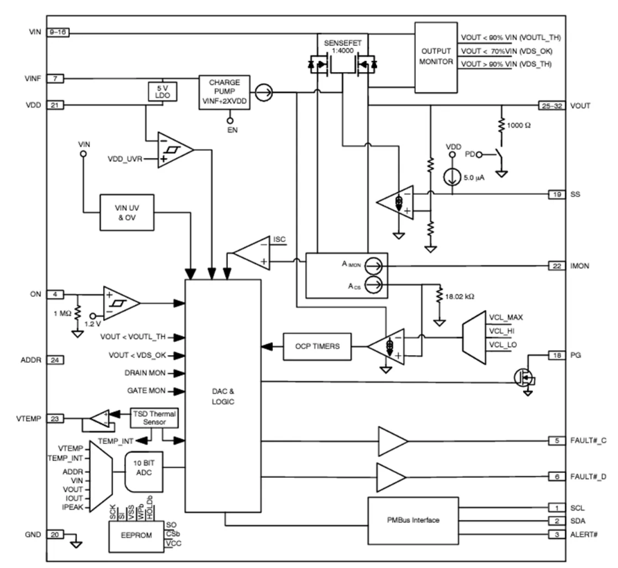
簡化框圖
關鍵特性
- 強大的功率處理能力:具備高達80 A的峰值輸出電流和50 A的連續(xù)輸出電流,輸入電壓工作范圍為5至18 V,在待機狀態(tài)下可承受高達30 V的電壓。
- 靈活的控制特性:可通過引腳斷言和/或PMBus進行控制,支持外部軟啟動編程,具備可編程的輸入欠壓警告和過壓故障保護,以及可編程的過流保護(OCP)級別和定時器。
- 出色的并行操作性能:支持多設備并行操作,在并行操作中具有良好的電流平衡能力,可實現(xiàn)軟啟動電流平衡。
- 全面的保護功能:擁有過溫關機、內部FET健康診斷、軟啟動電流限制和過度軟啟動持續(xù)時間保護等功能,還能記錄故障事件和峰值電流,并提供可編程的自動重試/鎖存關閉選項。
- 精準的遙測功能:符合PMBus 1.4標準,具備±2%的IMON精度(在30 A及以上),采用10位ADC對輸出電流、輸入電壓、輸出電流峰值、輸出電壓和溫度進行測量。
引腳功能與參數(shù)
引腳連接與功能
| NCP81428的引腳眾多,每個引腳都有其特定的功能。例如,SCL和SDA用于PMBus串行通信,ON為使能輸入,F(xiàn)AULT#_C和FAULT#_D用于主從設備之間的故障通信等。詳細的引腳功能描述如下表所示: | Pin No. | Symbol | Description |
|---|---|---|---|
| 1 | SCL | PMBus serial clock.Short to GND if not used. | |
| 2 | SDA | PMBus serial data input/output. Pull-up to 3.3 V if not used. | |
| 3 | ALERT# | ALERT pin is an Open drain output. A logic low alert signal of the PMBus interface. | |
| 4 | ON | Active high, enable input. | |
| 5 | FAULT#_C | Active low Fault communication pin in parallel applcation between master and slave devices. Connect FAULT#_C pins together in parallel applications. This pin is an output on the master and an input on the slave. | |
| 6 | FAULT#D | Active low Fault communication pin in parallel applcation between master and slave devices. Connect FAULT#_D pins together in parallel application. | |
| 7 | VINF | Control circuit power supply input.Connecto VIN pins through an RC fiter | |
| 8 | NC1 | Do not connect to this pin. Leave floating. | |
| 9 | VINO9 | Input of high current output switch (MOSFET drain connection). | |
| 10 | VIN10 | Input of high current output switch (MOSFET drain connection). | |
| 11 | VIN11 | Input of high current output swith (MOSFET drain connection). | |
| 12 | VIN12 | Input of high current output switch (MOSFET drain connection). | |
| 13 | VIN13 | Input of high current output switch (MOSFET drain connection). | |
| 14 | VIN14 | Input of high current output switch (MOSFE drain connection). | |
| 15 | VIN15 | Input of high current output swith (MOSFET drain connection). | |
| 16 | VIN16 | Input of high current output switch (MOSFET drain connection). | |
| 17 | NC2 | Do not connect to this pin. Leave floating. | |
| 18 | VTEMP | Analog temperature monitoring. Connect all VTEMP pins together in parallel applications. | |
| 19 | SS | Soft-start time programming pin. Connect a capacitor to this pin to set the soft-start time. The internal circuit controls the slew rate of the output voltage at turn-on. Connect all Ss pins together in parallel applications. | |
| 20 | GND | Ground | |
| 21 | VDD | Internal linear regulated supply output. Place a capacitor with a value of 4.7 uF or greater on this pin to maintain accuracy. | |
| 22 | IMON | Analog current monitor output,Connect a 2k resistor between pin and ground. A proportional current to the output current develops a voltage across the resistor. Connect all IMON pins together in parallel applications. | |
| 23 | PG | Power God, Open Drain output pin. Can be connected to VDD with a 100 kQ pull-up resistor. | |
| 24 | ADDR | PMBus address-setting pin. Connect a resistor from this pin to GND to set the device address. | |
| 25 | VOUT25 | Output of high current output switch (MOSFET source connection) | |
| 26 | VOUT26 | Output of high current output switch (MOSFET source connection). | |
| 27 | VOUT27 | Output of high current output switch (MOSFET source connection). | |
| 28 | VOUT28 | Output of high current output switch (MOSFET source connection). | |
| 29 | VOUT29 | Output of high current output switch (MOSFET source connection). | |
| 30 | VOUT30 | Output of high current output switch (MOSFET source connection). | |
| 31 | VOUT31 | Output of high current output switch (MOSFET source connection). | |
| 32 | VOUT32 | Output of high current output switch (MOSFET source connection). | |
| 33 | VIN33 | Input of high current output swith (MOSFET drain connection). |
電氣參數(shù)
NCP81428的電氣參數(shù)在不同的工作條件下有明確的規(guī)定。典型值是在 $T{J}=25^{\circ} C$,$VIN=VINF=12.0 ~V$,$V{ON}=3.3 ~V$,$C{VINF}=0.1 \mu F$,$C{VDD}=4.7uF$,$C{SS}=100 nF$ 的條件下測量得到的,而最小/最大值在 $6 ~V ≤VIN ≤18 ~V$,$-40^{\circ} C ≤T{J} \leq+125^{\circ} C$ 的范圍內有效。以下是一些關鍵電氣參數(shù)的示例:
- VINF輸入電流:在 $VON > 1.3 V$ 且無負載的情況下,工作電流為9.5 - 14 mA。
- VDD調節(jié)器:輸出電壓在1 mA < IVINF <10 mA,6 V < VINF < 18 V的條件下為4.7 - 5.3 V。
- ON輸入:上升開關導通閾值為1.10 - 1.30 V,開關導通延遲定時器為0.6 - 1.4 ms。
- IMON輸出:在不同的輸出電流條件下,精度有所不同,例如在IOUT = 30A,VIN = 12V,$T_{J} = 25^{\circ} C$ 時,精度為 -2% 至 +2%。
工作模式與配置
主從初始化與狀態(tài)機
NCP81428在主從配置中有特定的初始化流程和狀態(tài)機。上電后,當LDO輸出超過VDD UVLO閾值時,設備將默認值加載到操作寄存器中,然后讀取地址電阻(RADDR),以確定設備是主設備、從設備還是單設備,以及是否使用雙線接口(TWI)進行數(shù)據(jù)傳輸。
主設備響應ON引腳的高電平或PMBus命令來啟用,啟用后可進行自動校準(Auto - Cal)或數(shù)據(jù)傳輸。在數(shù)據(jù)傳輸過程中,F(xiàn)AULT#_C和FAULT#_D分別作為時鐘和數(shù)據(jù)信號,主設備向從設備傳輸數(shù)據(jù)。如果數(shù)據(jù)傳輸失敗,主設備會嘗試3次,若仍失敗,則根據(jù)工廠設置選擇繼續(xù)使用默認值或關閉設備。
系統(tǒng)配置
| NCP81428提供了多種系統(tǒng)配置方式,包括單設備配置、主從配置等。在主從配置中,最多可連接6個從設備。不同的配置方式通過ADDR引腳的電阻值來選擇,以實現(xiàn)不同的功能,如啟用或禁用NVM數(shù)據(jù)傳輸、PMBus通信等。以下是一些常見的配置示例: | 配置類型 | 描述 | 啟用方法 | PMBus | TWI | ADDR Pin Resistor |
|---|---|---|---|---|---|---|
| 單設備 | ON和/或SW | 是 | 否 | 20.0K NVM Data Transfer Disabled | ||
| 主設備 | ON和/或SW | 是 | 僅用于故障通信 | 9.31K,14.3K NVM Data Transfer Enabled 20.0K NVM Data Transfer Disabled | ||
| 單或多從設備 | FAULT#_C pulled up by Master | 是 | 26.7K to 73.2K NVM Data Transfer Enabled 86.6Kto 182K NVM Data Transfer Disabled | |||
| 單或多從設備 | - | 否 | Pulled to VDD (NVM Data Transfer Disabled) Shorted to GND (NVM Data Transfer Enabled) |
保護功能
電流限制與軟啟動
在啟動過程中,NCP81428的電流限制取決于輸入電壓(VIN)和輸出電壓(VOUT)的相對水平。當VIN < 13.2 V時,不同VOUT/VIN比例下的電流限制不同,例如在0 < VOUT < 0.4xVIN時,典型電流限制為7.5 A。如果電流限制條件持續(xù)時間超過 $t{CL _ REG}$,設備將鎖存關閉,若處于自動重試模式,則在 $t{DLY _ RETRY}$ 后嘗試重新軟啟動。
短路檢測與過流保護
NCP81428內置了高速電流感應SCP放大器,能夠快速響應短路故障,在檢測到故障后的 $t_{SC}$ 時間內開始拉低柵極電壓。設備提供了三個可編程的過流保護級別(OCP),每個級別都可以設置去抖時間和復位定時器,以確保準確檢測過流故障。
過溫保護與FET故障檢測
設備通過內部熱傳感器監(jiān)測芯片溫度,當溫度超過過熱警告閾值時,會通知主機采取相應措施;若超過過熱關機故障閾值,設備將關閉。此外,NCP81428還具備FET故障檢測功能,可檢測VIN到VOUT短路、GATE到VIN短路和GATE泄漏等故障,并根據(jù)故障類型采取相應的保護措施。
應用電路與設計指南
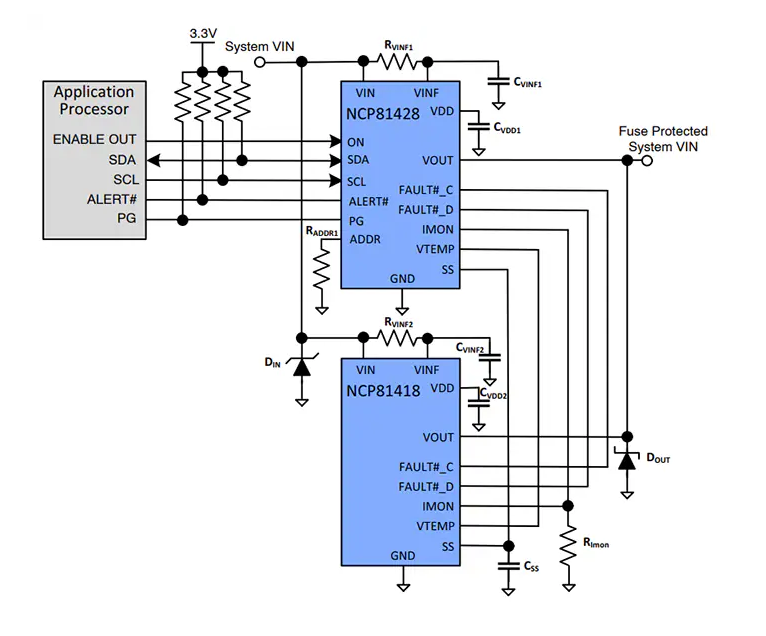
應用電路組件
| NCP81428的應用電路需要一些外部組件來確保其正常工作,以下是一些主要組件的信息: | Component | Manufacturer | Part Number | Value | Case Size | Voltage Rating |
|---|---|---|---|---|---|---|
| RVINF | Vishay | CRCW06031ROOFKEA | 1 | 0603 | 75V | |
| CVINF | Murata | 0603YC104KAT2A | 0.1pF | 0603 | 16V | |
| CvDD | Murata | GRM188C81E475KE11D | 4.7uF | 0603 | 25V | |
| Rimon | KOA Speer | RK73H1JTTD2001F | 2kg | 0603 | 75V | |
| Css | Murata | 0603YC104KAT2A | 0.1 pF | 0603 | 16V | |
| DIN | LittleFuse | SMBJ13A | Clamping Voltage = 21.5 V, Peak Current = 28 A | DO-214AA, 3.30 mm x4.06 mm | Vr=13V | |
| DoUT | onsemi | MBR2045EMFST3G | 20A | 8-SOFL,5mmx6mm | 45V |
瞬態(tài)電壓抑制
熱插拔eFuse容易受到電流突然中斷的影響,輸入電纜電感會在設備輸入產生正電壓瞬變尖峰,輸出電感會在輸出產生負電壓尖峰。為了抑制這些尖峰,需要使用外部TVS二極管和二極管進行鉗位。用戶可以使用公式 $V{Spike }=V{D C}+I_{OUT } × \sqrt{(L / C)}$ 大致估算尖峰電壓的大小。
總結
onsemi的NCP81428是一款功能強大、性能卓越的熱插拔智能保險絲,它在保護電路免受各種異常狀況影響的同時,還提供了靈活的配置選項和精準的遙測功能。無論是在服務器、數(shù)據(jù)存儲、基站還是工業(yè)應用中,NCP81428都能為電子設備的穩(wěn)定運行提供可靠的保障。電子工程師在設計相關電路時,可以充分利用NCP81428的特性,提高產品的性能和可靠性。你在使用類似產品的過程中遇到過哪些問題呢?歡迎在評論區(qū)分享你的經(jīng)驗和見解。
-
保險絲
+關注
關注
4文章
671瀏覽量
46997 -
熱插拔
+關注
關注
2文章
273瀏覽量
41150
發(fā)布評論請先 登錄
保險絲的分類/保險絲的性能和參數(shù)
怎么選保險絲規(guī)格
TPS25984可堆疊電子保險絲技術解析與應用指南
TPS25983 熱插拔電子保險絲技術解析與應用指南
NCP81418熱插拔智能保險絲技術解析與應用指南
深入解析NCP1345:高性能準諧振反激控制器的卓越之選


 工商網(wǎng)監(jiān)
評論