 【產品測試】利用設計網關的 IP 內核在 Xilinx VCK190 評估套件上加速人工智能應用

Xilinx 的 Versal AI Core 系列器件旨在解決獨特且最困難的 AI 推理問題,方法是使用高計算效率 ASIC 級 AI 計算引擎和靈活的可編程結構來構建具有加速器的 AI 應用,從而最大限度地提高任何給定工作負載的效率,同時提供低功耗和低延遲。
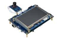
Versal AI Core 系列VCK190 評估套件采用VC1902器件,該器件在產品組合中具有最佳的 AI 性能。該套件專為需要高吞吐量 AI 推理和信號處理計算性能的設計而設計。VCK190 套件的計算能力是當前服務器級 CPU 的 100 倍,并具有多種連接選項,是從云到邊緣的各種應用的理想評估和原型設計平臺。
 圖 1:賽靈思 Versal AI 內核系列 VCK190 評估套件。(圖片來源:AMD, Inc)
VCK190 評估套件的主要特性
- 板載 Versal AI 核心系列設備
- 用于前沿應用開發的最新連接技術
- 協同優化工具和調試方法
利用賽靈思 Versal AI 內核系列器件實現 AI 接口加速
 圖 2:賽靈思 Versal AI 內核 VC1902 ACAP 器件框圖。(圖片來源:AMD, Inc)
Versal? AI Core 自適應計算加速平臺 (ACAP) 是一款高度集成的多核異構設備,可在硬件和軟件級別動態適應各種 AI 工作負載,使其成為 AI 邊緣計算應用或云加速器卡的理想選擇。該平臺集成了用于嵌入式計算的下一代標量引擎、用于硬件靈活性的自適應引擎,以及由 DSP 引擎和用于推理和信號處理的革命性 AI 引擎組成的智能引擎。其結果是一個適應性強的加速器,其性能、延遲和能效超過了傳統 FPGA 和 GPU 的性能、延遲和能效,適用于 AI/ML 工作負載。
Versal ACAP 平臺亮點
VCK190 人工智能推理性能
與當前服務器級 CPU 相比,VCK190 能夠提供超過 100 倍的計算性能。下面是基于 C32B6 DPU 內核的 AI 引擎實現的性能示例,批處理 = 6。有關 VCK190 上各種神經網絡樣本的吞吐量性能(以幀/秒或 fps 為單位),DPU 以 1250 MHz 運行,請參閱下表。
| | No | Neural Network | Input Size | GOPS | Performance (fps) (Multiple thread) |
| ---- | -------------------------- | ------------ | ------ | ------------------------------------- |
| 1 | face_landmark | 96x72 | 0.14 | 24605.3 |
| 2 | facerec_resnet20 | 112x96 | 3.5 | 5695.3 |
| 3 | inception_v2 | 224x224 | 4 | 1845.8 |
| 4 | medical_seg_cell_tf2 | 128x128 | 5.3 | 3036.3 |
| 5 | MLPerf_resnet50_v1.5_tf | 224x224 | 8.19 | 2744.2 |
| 6 | RefineDet-Medical_EDD_tf | 320x320 | 9.8 | 1283.6 |
| 7 | tiny_yolov3_vmss | 416x416 | 5.46 | 1424.4 |
| 8 | yolov2_voc_pruned_0_77 | 448x448 | 7.8 | 1366.0 |
Table 1: Example of VCK190 AI Inference performance.
See more detail of VCK190 AI performance from Vitis AI Library User Guide (UG1354), r2.5.0 at https://docs.xilinx.com/r/en-US/ug1354-xilinx-ai-sdk/VCK190-Evaluation-Board
How Design Gateway's IP cores accelerate AI application performance?
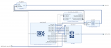
Design Gateway's IP Cores are designed to handle Networking and Data Storage protocol without need for CPU intervention. This makes it ideal to fully offload CPU systems from complicated protocol processing and which enables them to utilize most of their computing power for AI applications including AI inference, pre and post data processing, user interface, network communication and data storage access for the best possible performance.
 Figure 3: Block diagram of example an AI Application with Design Gateway's IP Cores. (Image source: Design Gateway)
Design Gateway's TCP Offload Engine IP (TOExxG-IP) performance
Processing high speed, high throughput TCP data streams over 10GbE or 25GbE by traditional CPU systems needs more than 50% of CPU time which reduces overall performance of AI applications. According to 10G TCP performance test on Xilinx's MPSoC Linux systems, CPU usage during 10GbE TCP transmission is more than 50%, TCP send and receive data transfer speed could be achieved just around 40% to 60% of 10GbE speed or 400 MB/s to 600 MB/s.
By implementing Design Gateway's TOExxG-IP Core, CPU usage for TCP transmission over 10GbE and 25GbE can be reduced to almost 0% while ethernet bandwidth utilization can be achieved close to 100%. This allows the sending and receiving of data over the TCP network directly by pure hardware logic and be fed into the Versal AI Engine with minimum CPU usage and the lowest possible latency. Figure 4 below shows the CPU usage and TCP transmission speed comparison between TOExxG-IP and MPSoC Linux systems.
 Figure 4: Performance comparison of 10G/25G TCP transmission by MPSoC Linux systems and Design Gateway's TOExxG-IP Core. (Image source: Design Gateway)
Design Gateway’s TOExxG-IP for Versal devices
 Figure 5: TOExxG-IP systems overview. (Image source: Design Gateway)
The TOExxG-IP core implements the TCP/IP stack (in hardwire logic) and connects with Xilinx’s EMAC Hard IP and Ethernet Subsystem module for the lower-layer hardware interface with 10G/25G/100G Ethernet speed. The user interface of the TOExxG-IP consists of a Register interface for control signals and a FIFO interface for data signals. The TOExxG-IP is designed to connect with Xilinx's Ethernet subsystem through the AXI4-ST interface. The clock frequency of the user interface depends on the Ethernet interface speed (e.g., 156.625 MHz or 322.266 MHz).
TOExxG-IP’s features
- Full TCP/IP stack implementation without need of the CPU
- Supports one session with one TOExxG-IP
- Multi-session can be implemented by using multiple TOExxG-IP instances
- Support for both Server and Client mode (Passive/Active open and close)
- Supports Jumbo frame
- Simple data interface by standard FIFO interface
- Simple control interface by single port RAM interface
FPGA resource usages on the XCVC1902-VSVA2197-2MP-ES FPGA device are shown in Table 2 below.
| | Family | Example Device | Fmax (MHz) | CLB Regs | CLB LUTs | Slice | IOB | BRAMTile^1^ | URAM | Design Tools |
| ---------------- | -------------------------- | ------------ | ---------- | ---------- | ------- | ----- | -------------- | ------ | -------------- |
| Versal AI Core | XCVC1902-VSVA2197-2MP-ES | 350 | 11340 | 10921 | 2165 | - | 51.5 | - | Vivado2021.2 |
Table 2: Example Implementation Statistics for Versal device.
More details of the TOExxG-IP are described in its datasheet which can be downloaded from Design Gateway’s website at the following links:
Design Gateway's NVMe Host Controller IP performance
NVMe Storage interface speed with PCIe Gen3 x4 or PCIe Gen4 x4 has data rates up to 32 Gbps and 64 Gbps. This is three to six times higher than 10GbE Ethernet speed. Processing complicated NVMe storage protocol by the CPU to achieve the highest possible disk access speed requires more CPU time than TCP protocol over 10GbE.
Design Gateway solved this problem by developing the NVMe IP core that is able to run as a standalone NVMe host controller, able to communicate with an NVMe SSD directly without the CPU. This enables a high efficiency and performance of the NVMe PCIe Gen3 and Gen4 SSD access, which simplifies the user interface and standard features for ease of usage without needing knowledge of the NVMe protocol. NVMe PCIe Gen4 SSD performance can achieve up to a 6 GB/s transfer speed with NVMe IP as shown in Figure 6.
 Figure 6: Performance comparison of NVMe PCIe Gen3 and Gen4 SSD with Design Gateway's NVMe-IP Core. (Image source: Design Gateway)
Design Gateway's NVMe-IP’s for Versal devices
 圖 7:NVMe-IP 系統概述。(圖片來源:設計網關)
NVMe-IP的功能
- 能夠實現應用層、事務層、數據鏈路層和物理層的某些部分,無需CPU或外部DDR存儲器即可訪問NVMe SSD
- 與賽靈思 PCIe 第 3 代和第 4 代硬 IP 配合使用
- 能夠利用BRAM和URAM作為數據緩沖區,而無需外部存儲器接口
- 支持六個命令:識別、關機、寫入、讀取、SMART 和刷新(提供可選的附加命令支持)
XCVC1902-VSVA2197-2MP-E-S FPGA 器件上的 FPGA 資源使用情況如表 2 所示。
| | 家庭 | 示例設備 | 最大頻率 (兆赫) | 負載均衡注冊 | 負載均衡 LUT | 片 | IOB | 布拉姆蒂勒^1^ | 烏蘭 | 設計工具 |
| ---------------- | -------------------------- | ------------------- | -------------- | -------------- | ------ | ----- | ---------------- | ------ | ------------ |
| Versal AI Core | XCVC1902-VSVA2197-2MP-ES | 375 | 6280 | 3948 | 1050 | - | 4 | 8 | 萬歲2022.1 |
表 3:Versal 設備的實現統計信息示例。
有關 Versal 器件的 NVMe-IP 的更多詳細信息,請參見其數據表,可通過以下鏈接從 Design Gateway 的網站下載:
結論
TOExxG-IP 和 NVMe-IP 內核都可以通過將 CPU 系統從計算和內存密集型協議(如 TCP 和 NVMe 存儲協議)中完全卸載來幫助加速 AI 應用程序性能,這對于實時 AI 應用程序至關重要。這使得賽靈思的 Versal AI Core 系列器件能夠執行 AI 推理和高性能計算應用,而不會出現網絡和數據存儲協議處理的瓶頸或延遲。
VCK190 評估套件和 Design Gateway 的網絡和存儲 IP 解決方案可在 Xilinx 的 Versal AI Core 器件上以盡可能低的 FPGA 資源使用量和極高的能效在 AI 應用中實現最佳性能。
-
網關
+關注
關注
9文章
6767瀏覽量
56251
發布評論請先 登錄
淺談人工智能(2)

人工智能+工業物聯網網關有什么功能作用
探索CY8CKIT - 062S2 - AI PSoC? 6人工智能評估套件
探索AMD XILINX Versal Prime Series VMK180評估套件,開啟硬件創新之旅
Jtti設計網絡態勢感知測試海外VPS:安全評估與實施方案
利用超微型 Neuton ML 模型解鎖 SoC 邊緣人工智能
AI 邊緣計算網關:開啟智能新時代的鑰匙?—龍興物聯
挖到寶了!人工智能綜合實驗箱,高校新工科的寶藏神器
挖到寶了!比鄰星人工智能綜合實驗箱,高校新工科的寶藏神器!
在AMD Versal自適應SoC上使用QEMU+協同仿真示例
是德示波器DSOX6002A在人工智能芯片測試中的應用
超小型Neuton機器學習模型, 在任何系統級芯片(SoC)上解鎖邊緣人工智能應用.
固態電池測試套件
STM32N6570-DK:邊緣人工智能開發的全能探索板
Cognizant將與NVIDIA合作部署神經人工智能平臺,加速企業人工智能應用


 工商網監
工商網監
評論